Section 2 Setup
2-28
2.3.10 The call processing port
The
Call Proc I/O
connector (D-SUB, 15 pins) on the rear panel of MT8820A is
used to input/output signals related to the call-processing test.
Pin assignment varies, depending on the measurement software. Check the meas-
urement software to be used.
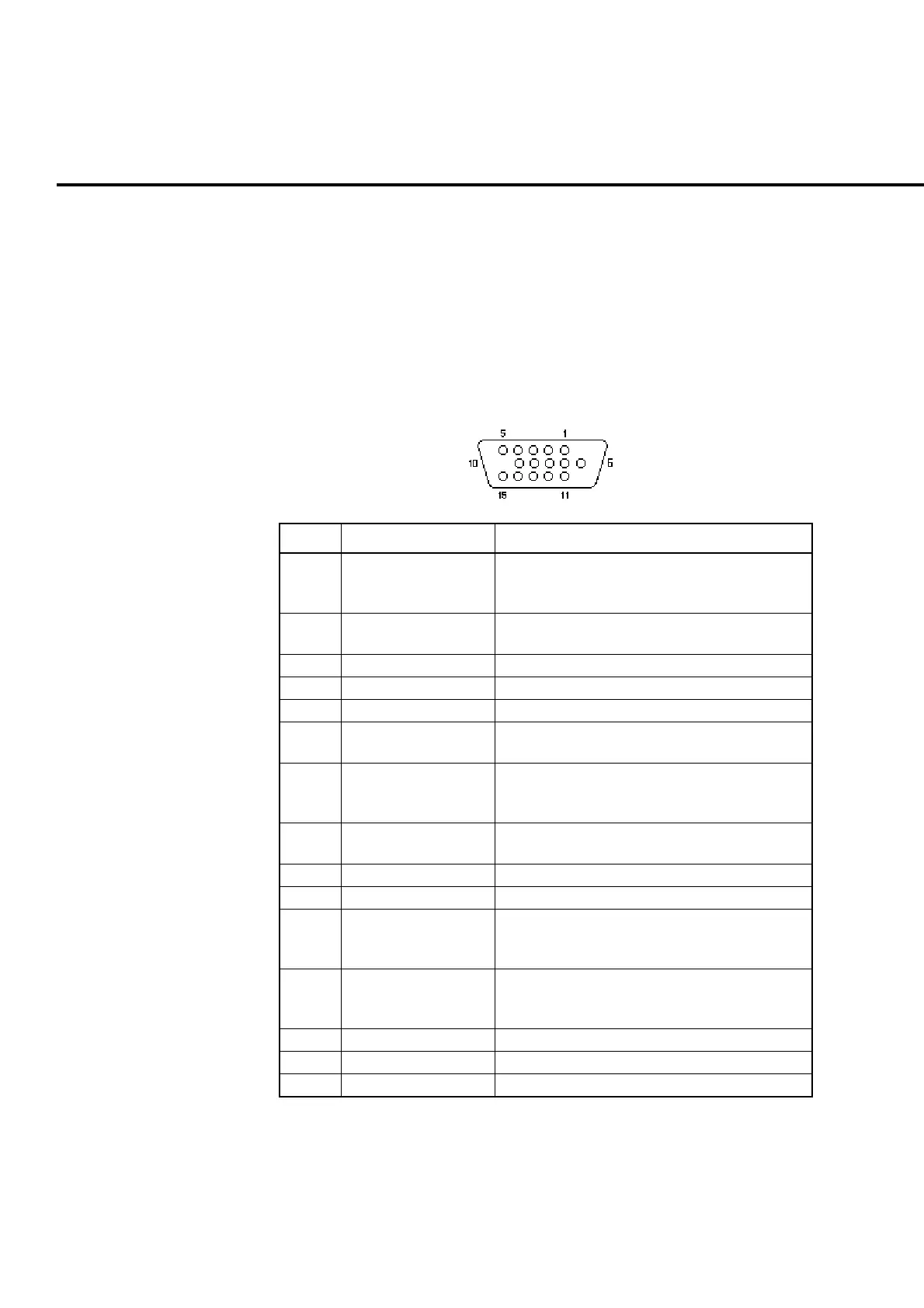
Table 2-3-10-1 Signal assignment of Call Proc I/O connector
When using W-CDMA, GSM or PDC measurement software
Pin No Signal name Description
1 BER_DAT_IN Input the data for BER measurement. The
phone inputs the demodulated data of the TTL
or CMOS level
2 BER_DAT_OUT Outputs the demodulated data of the CMOS
level.
3 DSUB15_RSV1 Reserved
4 DSUB15_RSV4 Reserved
5 DSUB15_RSV7 Reserved
6 FRAME_TRG_OUT
Outputs the trigger signal of the CMOS level in
a frame period.
7 BER_CLK_IN Input the clock signal for BER measurement.
Input the data clock of the TTL or CMOS level,
demodulated by the tested terminal.
8 BER_CLK_OUT Outputs the demodulated data clock of the
CMOS level.
9 DSUB15_RSV2 Reserved
10 DSUB15_RSV5 Reserved
11 SYNC IN Input the synchronization signal of the TTL or
CMOS level from the master unit, when two
units of MT8820A are synchronously operated.
12 SYNC OUT
Outputs the synchronization signal of the CMOS
level to the slave unit, when two units of
MT8820A are synchronously operated.
13 GND Ground
14 DSUB15_RSV3 Reserved
15 DSUB15_RSV6 Reserved