Memory Interface
ARM DDI 0210C Copyright © 2001, 2004 ARM Limited. All rights reserved. 3-19
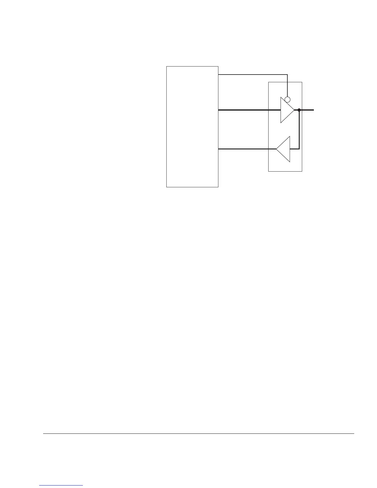
Figure 3-14 External connection of unidirectional buses
Bidirectional data bus
When BUSEN is LOW, the buffer between DIN[31:0] and D[31:0] is disabled. Any
data presented on DIN[31:0] is ignored. Also, when BUSEN is LOW, the value on
DOUT[31:0] is forced to
0x00000000
.
When the ARM7TDMI processor is reading from memory DIN[31:0] is acting as an
input. During write cycles the ARM7TDMI core must output data. During phase 2 of
the previous cycle, the signal nRW is driven HIGH to indicate a write cycle. During the
actual cycle, nENOUT is driven LOW to indicate that the processor is driving D[31:0]
as an output. Figure 3-15 on page 3-20 shows the bus timing with the data bus enabled.
Figure 3-16 on page 3-20 shows the circuit that exists in the processor for controlling
exactly when the external bus is driven out.
ARM7TDMI
PAD
DOUT[31:0]
XDATA[31:0]
DIN[31:0]
nENOUT