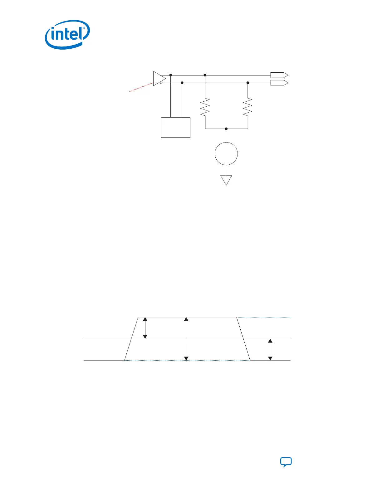
Figure 169. Transmitter Buffer
TX
V
CM
To Serial Data
Output Pins
(tx_serial_data)
Programmable
Pre-Emphasis
and VOD
Receiver
Detect
On-Chip
Termination
85Ω, 100Ω, OFF
R1*
R1*
R1* - Half of the actual on-chip termination selected.
5.1.1.2.1. High Speed Differential I/O
To improve performance, the Cyclone 10 GX transmitter uses a new architecture in the
output buffer—High Speed Differential I/O. You should select "High Speed Differential
I/O" for I/O standard of Cyclone 10 GX transmitter pin in Quartus Prime Assignment
Editor or QSF file.
5.1.1.2.2. Programmable Output Differential Voltage
You can program the differential output voltage (output swing) to handle different
channel losses and receiver requirements. There are 31 differential V
OD
settings up to
VCCT power supply level. The step size is 1/30 of the VCCT power supply level.
Figure 170. V
OD
(Differential) Signal Level
Differential Waveform
+V
P
V
OD
(Differential)
–V
N
V
OD
(Differential) = V
P
- V
N
0 V Differential
Related Information
For more information, refer to Cyclone 10 GX Pre-Emphasis and Output Swing
Settings
5. Cyclone 10 GX Transceiver PHY Architecture
UG-20070 | 2018.09.24
Intel
®
Cyclone
®
10 GX Transceiver PHY User Guide
Send Feedback
274