Figure 171. Receiver PMA Block Diagram
Receiver
PCS
Deserializer
Parallel Data
to FPGA Core
Parallel
Data
Serial
Data
Serial Clock
Receiver PMA
CDR
Serial
Data
Receiver
Buffer
Parallel Clock
Receiver Serial
Differential Input
Data
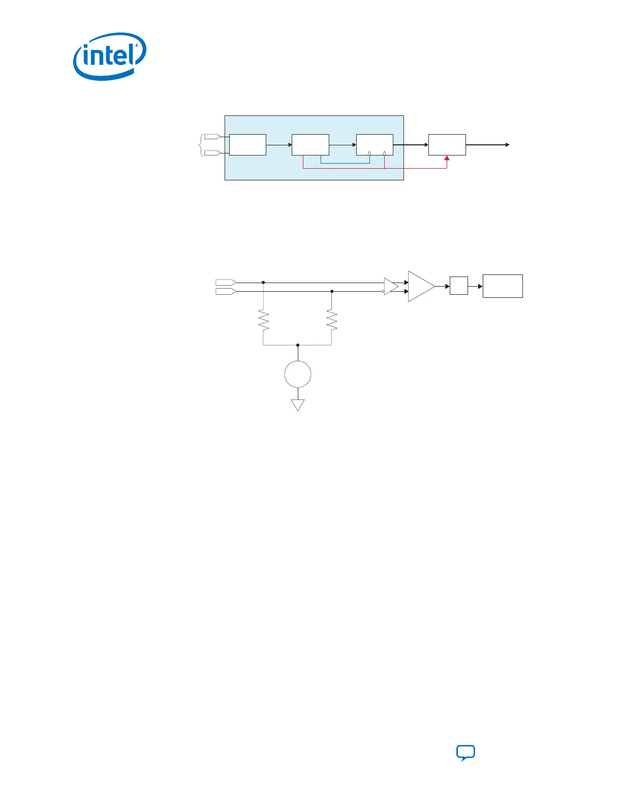
5.1.2.1. Receiver Buffer
The receiver input buffer receives serial data from rx_serial_data and feeds the
serial data to the clock data recovery (CDR) unit and deserializer.
Figure 172. Receiver Buffer
RX
V
CM
From Serial Data
Input Pins
(rx_serial_data)
VGA
CTLE
To CDR
RX
Termination
85Ω, 100Ω, OFF
R1* - Half of the actual on-chip termination selected
R1*
R1*
The receiver buffer supports the following features:
• Programmable common mode voltage (V
CM
)
• Programmable differential On-Chip Termination (OCT)
• Signal Detector
• Continuous Time Linear Equalization (CTLE)
• Variable Gain Amplifiers (VGA)
5.1.2.1.1. Programmable Common Mode Voltage (V
CM
)
The receiver buffer has on-chip biasing circuitry to establish the required V
CM
at the
receiver input.
The Quartus Prime software automatically chooses the optimal setting for RX V
CM
.
Note: On-chip biasing circuitry is available only if you select OCT. If you select external
termination, you must implement off-chip biasing circuitry to establish the V
CM
at the
receiver input buffer.
Manual V
CM
adjustment is not supported and is only adjusted by calibrations.
5. Cyclone 10 GX Transceiver PHY Architecture
UG-20070 | 2018.09.24
Intel
®
Cyclone
®
10 GX Transceiver PHY User Guide
Send Feedback
276