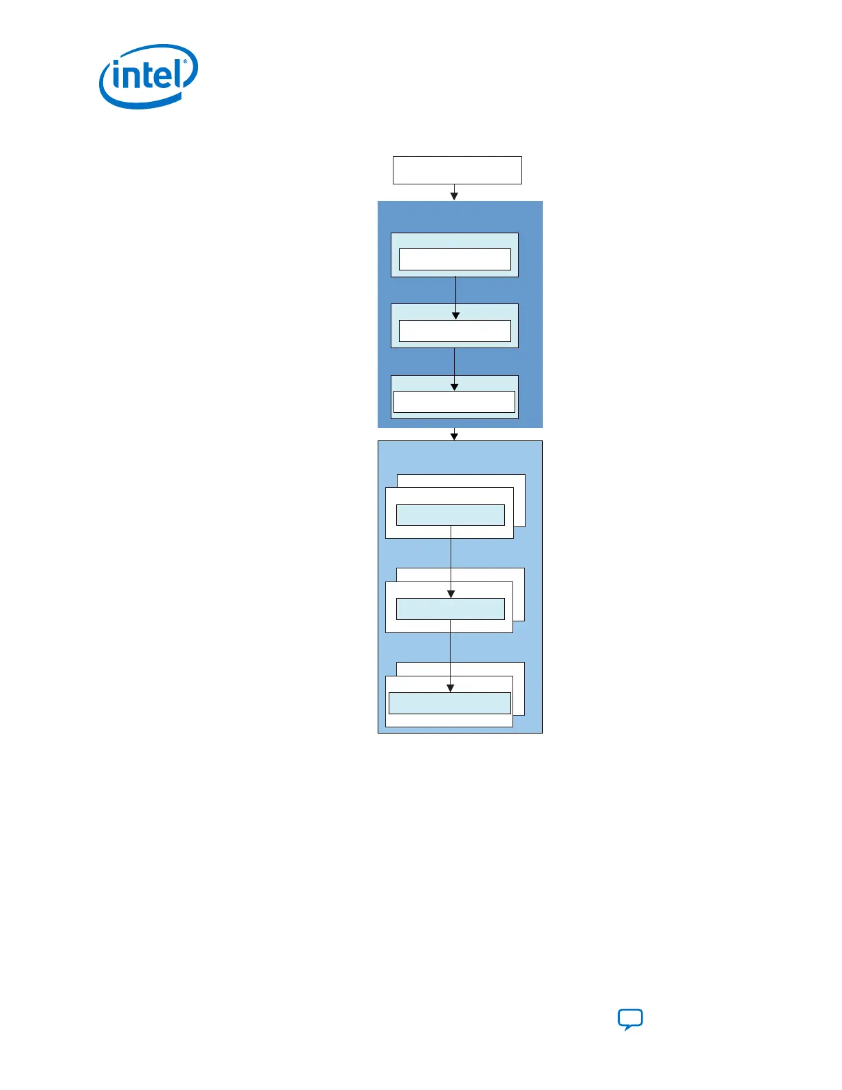
Figure 223. Power-up Calibration Sequence for PCIe Hard IP and non-PCIe Channels
Bank 1
Bank 2
ATX PLL Calibration
PCIe Channels Calibration
Non-PCIe Channels Calibration
Voltage Regulator (Vreg) Calibration for
All Transceiver Banks and Channels
Bank 1
Bank 2
fPLL Calibration
Bank 1
Bank 2
RX PMA and TX PMA Calibration (1), (2)
After All ATX PLLs Calibrated
After All fPLLs Calibrated
Hard IP 0
ATX PLL Calibration
Hard IP 0
fPLL Calibration
Hard IP 0
RX PMA and TX PMA Calibration (1), (2)
After All ATX PLL Calibrated
After All fPLL Calibrated
Notes:
(1) CDR/CMU PLL calibration is part of
RX PMA calibration.
(2) For power-up calibration, RX PMA
calibration happens before TX PMA
calibration.
7. Calibration