RL78/G1H CHAPTER 4 CPU ARCHITECTURE
R01UH0575EJ0120 Rev. 1.20 Page 37 of 920
Dec 22, 2016
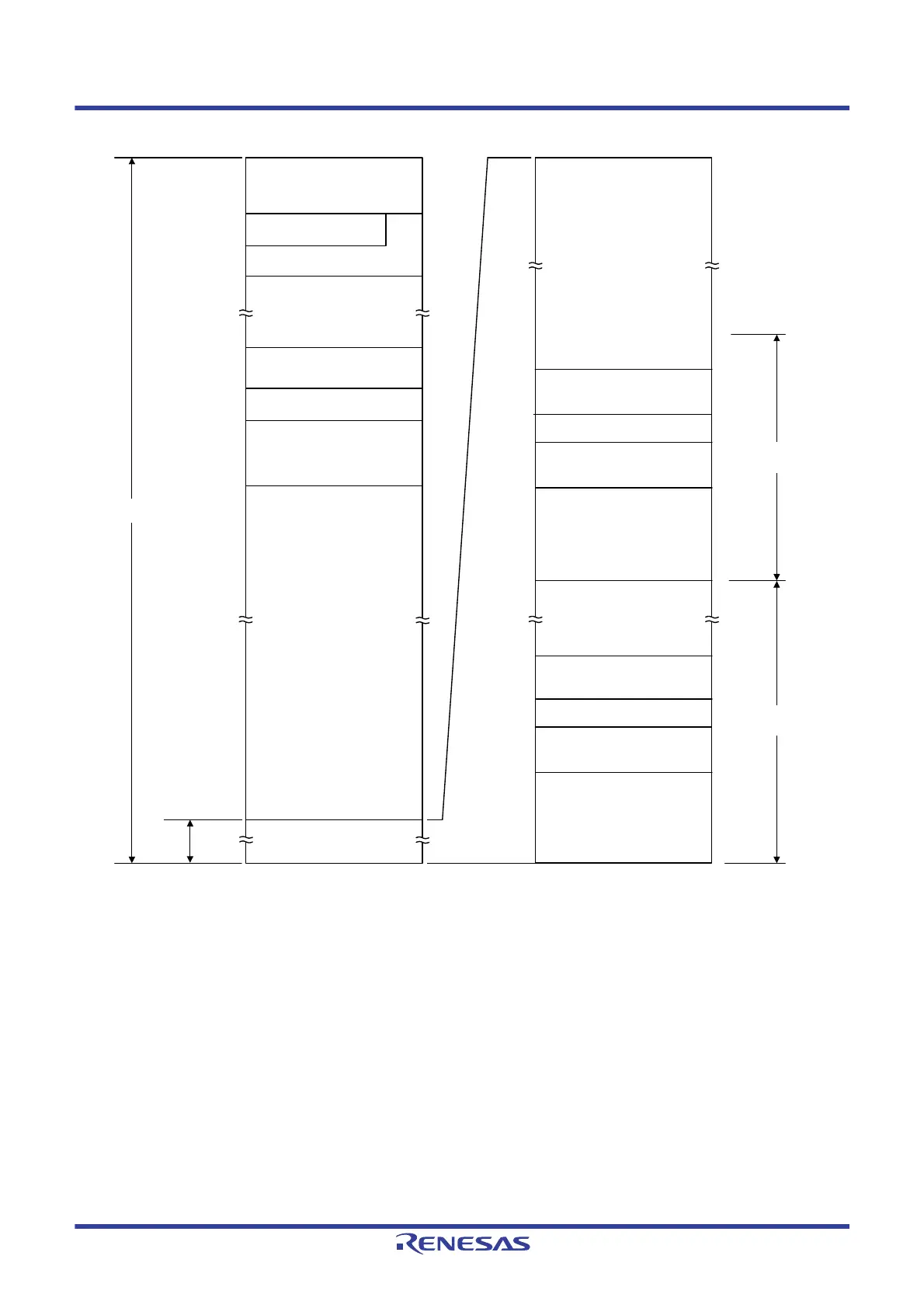
Figure 4 - 1 Memory Map (R5F11FLJ)
Note 1. Do not allocate RAM addresses which are used as a stack area, a data buffer, a branch destination of vector interrupt
processing, and a DTC transfer destination/transfer source to the area FFE20H to FFEDFH when performing self-
programming and rewriting the data flash memory.
Note 2. Instructions can be executed from the RAM area excluding the general-purpose register area.
Note 3. When boot swap is not used: Set the option bytes to 000C0H to 000C3H, and the on-chip debug security IDs to 000C4H
to 000CDH.
When boot swap is used: Set the option bytes to 000C0H to 000C3H and 010C0H to 010C3H, and the on-chip debug
security IDs to 000C4H to 000CDH and 010C4H to 010CDH.
Note 4. Writing boot cluster 0 can be prohibited depending on the setting of security (see 27.6 Security Settings).
Note 5. Use of the area FA300H to FA6FFH is prohibited when using the on-chip debugging trace function.
Caution While RAM parity error resets are enabled (RPERDIS = 0), be sure to initialize RAM areas where data access is to
proceed and the RAM area + 10 bytes when instructions are fetched from RAM areas, respectively.
Reset signal generation sets RAM parity error resets to enabled (RPERDIS = 0). For details, see 24.3.3 RAM parity
error detection function.
FFFFFH
FFEE0H
FFEDFH
F9F00H
F9EFFH
F3000H
F2FFFH
F1000H
F0FFFH
F0800H
F07FFH
F0000H
EFFFFH
40000H
3FFFFH
00000H
Data memory
space
Program
memory
space
FFF00H
FFEFFH
Special function register (SFR)
256 bytes
General-purpose register
32 bytes
RAM
Notes 1, 2
24 Kbytes
Mirror
27.75 Kbytes
Data flash memory
8 Kbytes
Reserved
Extended special function register
(2nd SFR)
2 Kbytes
Reserved
Code flash memory
256 Kbytes
00000H
01FFFH
010CEH
010CDH
010C4H
010C3H
010C0H
010BFH
01080H
0107FH
000CEH
000CDH
01000H
00FFFH
3FFFFH
000C4H
000C3H
000C0H
000BFH
00080H
0007FH
Boot cluster 0
Note 4
Boot cluster 1
Program area
Program area
CALLT table area
64 bytes
Vector table area
128 bytes
Option byte area
Note 3
4 bytes
CALLT table area
64 bytes
Vector table area
128 bytes
On-chip debug security
ID setting area
Note 3
10 bytes
Option byte area
Note 3
4 bytes
On-chip debug security
ID setting area
Note 3
10 bytes
 Loading...


