RL78/G1H CHAPTER 3 PIN FUNCTIONS
R01UH0575EJ0120 Rev. 1.20 Page 22 of 920
Dec 22, 2016
3.2 Functions other than port pins
Note This pin is used for connection between the MCU and RF transceiver. For details, refer to CHAPTER 2 CONNECTION
BETWEEN MCU AND RF TRANSCEIVER
.
Caution After reset release, the relationships between P40/TOOL0 and the operating mode are as follows.
For details, see 27.3 Programming Method.
Remark
A bypass capacitor about 0.1 μF must be connected for measures of noises and latch-up between VDD and VSS lines on
the shortest distance and with comparative thick wire.
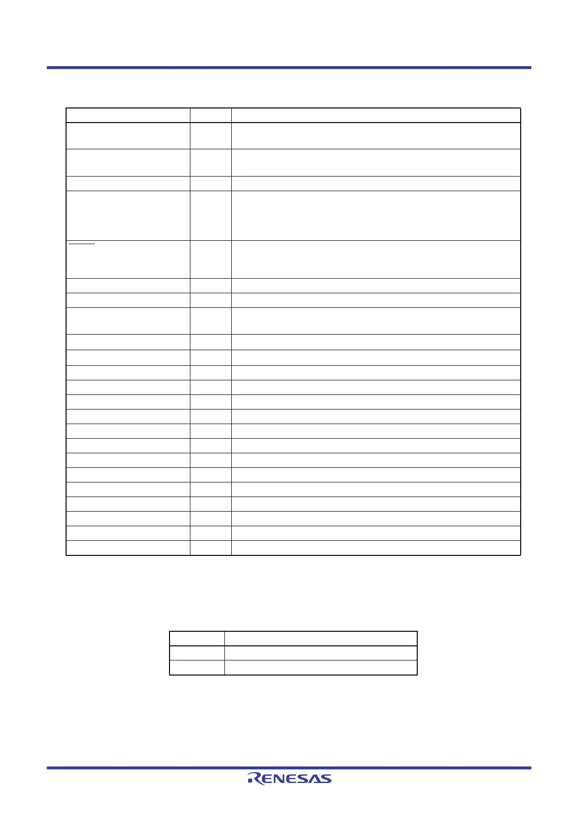
Function Name I/O Function
ANI0 to ANI2, ANI13, ANI14,
ANI19
Input
A/D converter analog input (see
Figure 13 - 30 Analog Input Pin Connection)
INTP0, INTP3
Note
, INTP4, INTP6,
INTP7, INTP9 to INTP11
Input
External interrupt request input
Valid edge specification: Rising edge, falling edge, or both rising and falling edges
PCLBUZ0, PCLBUZ1 Output Clock output/buzzer output
REGC
—
Pin for connecting regulator output stabilization capacitance for internal operation.
Connect this pin to V
SS via a capacitor (0.47 to 1 μF).
Also, use a capacitor with good characteristics, since it is used to stabilize internal
voltage.
RESET
Input
This is the active-low system reset input pin.
When the external reset pin is not used, connect this pin directly or via a resistor to
V
DD.
RxD1, RxD3 Input Serial data input pins of serial interface UART1 and UART3
TxD1, TxD3 Output Serial data output pins of serial interface UART1 and UART3
SCK10, SCK20
Note
, SCK21,
SCK30
I/O
Serial clock I/O pins of serial interface CSI10, CSI20, CSI21, and CSI30
SI10, SI20
Note
, SI21, SI30
Input
Serial data input pins of serial interface CSI10, CSI20, CSI21, and CSI30
SO10, SO20
Note
, SO21, SO30
Output
Serial data output pins of serial interface CSI10, CSI20, CSI21, and CSI30
SCLA0, SCLA1 I/O Serial clock I/O pins of serial interface IICA0 and IICA1
SDAA0, SDAA1 I/O Serial data I/O pins of serial interface IICA0 and IICA1
TI03 Input The pins for inputting an external count clock/capture trigger to 16-bit timer 03
TO03 Output Timer output pins of 16-bit timer 03
X1, X2 — Resonator connection for main system clock
EXCLK Input External clock input for main system clock
XT1, XT2 — Resonator connection for subsystem clock
EXCLKS Input External clock input for subsystem clock
V
DD — Positive power supply for all pins
AV
REFP Input A/D converter reference potential (+ side) input
AV
REFM Input A/D converter reference potential (- side) input
V
SS — Ground potential for all pins
TOOL0 I/O Data I/O for flash memory programmer/debugger
Table 3 - 2 Relationships Between P40/TOOL0 and Operation Mode After Reset Release
P40/TOOL0 Operating mode
V
DD Normal operation mode
0 V Flash memory programming mode
 Loading...


