RL78/G1H CHAPTER 17 EVENT LINK CONTROLLER (ELC)
R01UH0575EJ0120 Rev. 1.20 Page 541 of 920
Dec 22, 2016
17.3 Registers Controlling ELC
17.3.1 Event output destination select register n (ELSELRn) (n = 00, 03, 04, 07,
13, 16 to 23)
An ELSELRn register links each event signal to an operation of an event-receiving peripheral function (link
destination peripheral function) after reception.
Do not set multiple event inputs to the same event output destination (event receive side). The operation of the
event-receiving peripheral function will become undefined, and event signals may not be received correctly. In
addition, do not set the event link generation source and the event link output destination to the same function.
Set an ELSELRn register during a period when no event output peripheral functions are generating event
signals.
Table 17 - 1 lists the correspondence between ELSELRn registers and peripheral functions.
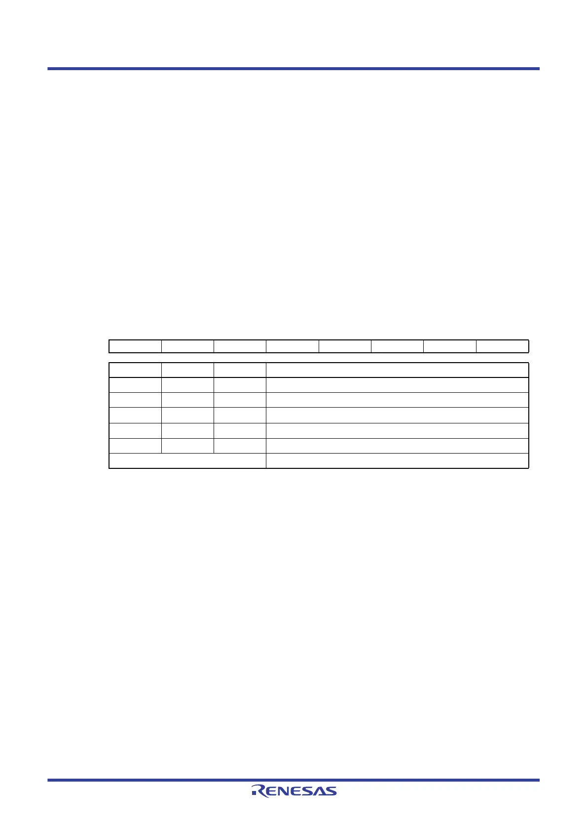
Figure 17 - 2 Format of Event output destination select register n (ELSELRn)
Note 1. To select the timer input of timer array unit 0 channel 0 as the link destination peripheral function, set the
operating clock for channel 0 to f
CLK using timer clock select register 0 (TPS0), set the noise filter of the TI00
pin to OFF (TNFEN00 = 0) using noise filter enable register 1 (NFEN1), and then set the timer output used
for channel 0 to an event input signal from the ELC using timer input select register 0 (TIS0).
Note 2. To select the timer input of timer array unit 0 channel 1 as the link destination peripheral function, set the
operating clock for channel 1 to f
CLK using timer clock select register 0 (TPS0), set the noise filter of the TI01
pin to OFF (TNFEN01 = 0) using noise filter enable register 1 (NFEN1), and then set the timer output used
for channel 1 to an event input signal from the ELC using timer input select register 0 (TIS0).
Address: F0300H (ELSELR00) to F0317H (ELSELR23) After reset: 00H R/W
Symbol76543210
ELSELRn 0 0 0 0 0 ELSELn2 ELSELn1 ELSELn0
ELSELn2 ELSELn1 ELSELn0 Event Link Selection
0 0 0 Event link disabled
0 0 1 Hardware trigger signal of A/D converter
010
Timer input of timer array unit 0 channel 0
Note 1
011
Timer input of timer array unit 0 channel 1
Note 2
1 0 0 Count source of timer RJ
Other than above Setting prohibited
 Loading...


