RL78/G1H CHAPTER 31 ELECTRICAL SPECIFICATIONS
R01UH0575EJ0120 Rev. 1.20 Page 895 of 920
Dec 22, 2016
Note 1. Excludes quantization error (±1/2 LSB).
Note 2. This value is indicated as a ratio (% FSR) to the full-scale value.
31.6.2 POR characteristics
Note 1. However, when the operating voltage falls while the LVD is off, enter STOP mode, or enable the reset status using the
voltage detection function or external reset pin before the voltage falls below the operating voltage range shown in
31.4
AC Characteristics
.
Note 2. Minimum time required for a POR reset when VDD exceeds below VPDR. This is also the minimum time required for a
POR reset from when V
DD exceeds below 0.7 V to when VDD exceeds VPOR while STOP mode is entered or the main
system clock (f
MAIN) is stopped through setting bit 0 (HIOSTOP) and bit 7 (MSTOP) in the clock operation status control
register (CSC).
(2) When reference voltage (+) = VDD (ADREFP0 = 0), reference voltage (‒) = VSS (ADREFM = 0),
target pin: ANI0 to ANI2, ANI13, ANI14, ANI19
(T
A = ‒40 to +85 °C, 1.8 V ≤ VDD ≤ 3.6 V, VSS = 0 V, Reference voltage (+) = VDD, Reference voltage (‒) = VSS)
Parameter Symbol Conditions MIN. TYP. MAX. Unit
Resolution RES 8 10 bit
Overall error
Note 1
AINL 10-bit resolution 1.8 V ≤ VDD ≤ 3.6 V 1.2 ±7.0 LSB
Conversion time t
CONV 10-bit resolution
Target pin: ANI0 to ANI2, ANI13, ANI14, ANI19
2.7 V ≤ VDD ≤ 3.6 V
3.1875
39 μs
1.8 V
≤ VDD ≤ 3.6 V 17 39 μs
Zero-scale error
Notes 1, 2
EZS 10-bit resolution 1.8 V ≤ VDD ≤ 3.6 V ±0.60 %FSR
Full-scale error
Notes 1, 2
EFS 10-bit resolution 1.8 V ≤ VDD ≤ 3.6 V ±0.60 %FSR
Integral linearity error
Note 1
ILE 10-bit resolution 1.8 V ≤ VDD ≤ 3.6 V ±4.0 LSB
Differential linearity error
Note
1
DLE 10-bit resolution 1.8 V ≤ VDD ≤ 3.6 V ±2.0 LSB
Analog input voltage V
AIN ANI0 to ANI2, ANI13, ANI14, ANI19 0 VDD V
(TA = ‒40 to +85 °C, VSS = 0 V)
Parameter Symbol Conditions MIN. TYP. MAX. Unit
Voltage detection threshold V
POR Voltage threshold on VDD rising 1.47 1.51 1.55 V
V
PDR
Voltage threshold on VDD falling
Note 1
1.46 1.50 1.54 V
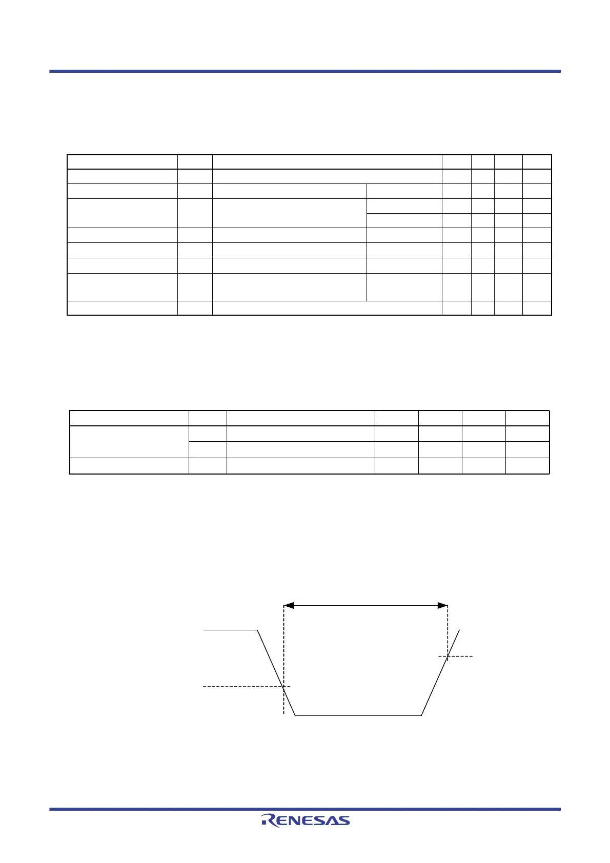
Minimum pulse width
Note 2
TPW
300 μs
TPW
VPOR
VPDR or 0.7 V
Supply voltage (V
DD)
 Loading...


