RL78/G1H CHAPTER 13 A/D CONVERTER
R01UH0575EJ0120 Rev. 1.20 Page 287 of 920
Dec 22, 2016
13.3.2 A/D converter mode register 0 (ADM0)
This register sets the conversion time for analog input to be A/D converted, and starts/stops conversion.
The ADM0 register can be set by a 1-bit or 8-bit memory manipulation instruction.
Reset signal generation clears this register to 00H.
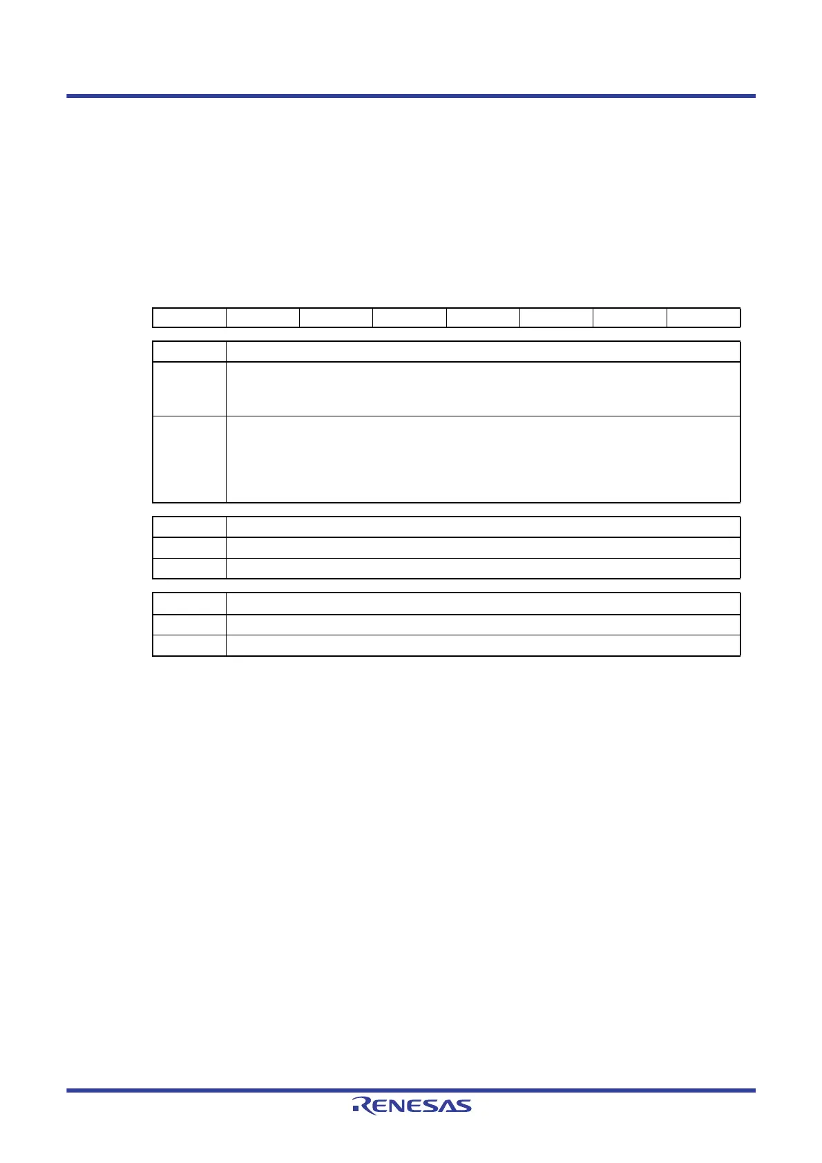
Figure 13 - 3 Format of A/D converter mode register 0 (ADM0)
Note 1. For details of the FR2 to FR0, LV1, LV0 bits, and A/D conversion, see Tables 13 - 3 to 13 - 6 A/D
Conversion Time Selection
.
Note 2. While in the software trigger mode or hardware trigger no-wait mode, the operation of the A/D voltage
comparator is controlled by the ADCS and ADCE bits, and it takes 1
μs from the start of operation for the
operation to stabilize. Therefore, when the ADCS bit is set to 1 after 1
μs or more has elapsed from the time
ADCE bit is set to 1, the conversion result at that time has priority over the first conversion result. Otherwise,
ignore data of the first conversion.
Caution 1. Change the FR2 to FR0, LV1, and LV0 bits while conversion is stopped (ADCS = 0, ADCE = 0).
Caution 2. Do not set the ADCS bit to 1 and the ADCE bit to 0 at the same time.
Caution 3. Do not change the ADCS and ADCE bits from 0 to 1 at the same time by using an 8-bit manipulation
instruction. Be sure to set these bits in the order described in 13.7 A/D Converter Setup Flowchart.
Address: FFF30H After reset: 00H R/W
Symbol<7>654321<0>
ADM0 ADCS ADMD
FR2
Note 1
FR1
Note 1
FR0
Note 1
LV1
Note 1
LV0
Note 1
ADCE
ADCS A/D conversion operation control
0 Stops conversion operation
[When read]
Conversion stopped/standby status
1 Enables conversion operation
[When read]
While in the software trigger mode: Conversion operation status
While in the hardware trigger wait mode: A/D power supply stabilization wait status +
conversion operation status
ADMD Specification of the A/D conversion channel selection mode
0 Select mode
1 Setting prohibited
ADCE
A/D voltage comparator operation control
Note 2
0 Stops A/D voltage comparator operation
1 Enables A/D voltage comparator operation
 Loading...


