generated. In this case, the results are not stored in the ADCR, ADCRH register.
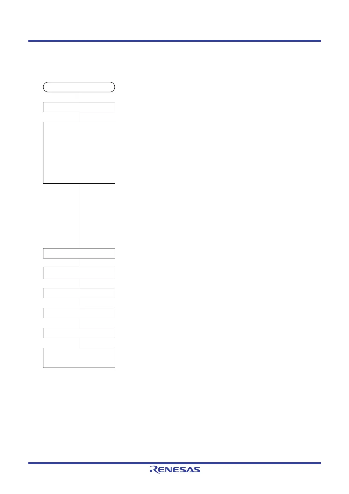
Start of setup
PER0 register setting
The ADCEN bit of the PER0 register is set (1), and supplying the clock starts.
• ADM0 register setting
• ADM1 register setting
• ADM2 register setting
• ADUL/ADLL register setting
• ADS register setting
• ADTES register setting
(The order of the settings is
irrelevant.)
Reference voltage stabilization
wait time count
ADCS bit setting
Start of A/D conversion
End of A/D conversion
The A/D conversion operations are performed.
Storage of conversion results in
the ADCR and ADCRH registers
ADCE bit setting
• ADM0 register
FR2 to FR0, LV1, and LV0 bits: These are used to specify the A/D conversion time.
• ADM1 register
ADTMD1 and ADTMD0 bits: These are used to specify the software trigger mode.
ADSCM bit: This is used to specify the one-shot conversion mode.
• ADM2 register
ADREFP0 and ADREFM bits: These are used to select for the reference voltage.
ADRCK bit: This is used to set the range for the A/D conversion result comparison
value generated by the interrupt signal to AREA 2.
ADTYP bit: This is used to specify 10-bit resolution.
• ADUL/ADLL register
These set ADUL to FFH and ADLL to 00H (initial values).
• ADS register
ADS4 to ADS0 bits: These are used to set to ANI0.
• ADTES register
ADTES1 and ADTES0 bits: AV
REFM/AVREFP
The ADCE bit of the ADM0 register is set (1), and the system enters the A/D
conversion standby status.
The reference voltage stabilization wait time (1 µs) is counted by the software.
After counting up to the reference voltage stabilization wait time B ends, the
ADCS bit of the ADM0 register is set (1), and A/D conversion starts.
The A/D conversion end interrupt (INTAD) is generated.
Note
The conversion results are stored in the ADCR and ADCRH registers.
 Loading...


