RL78/G1H CHAPTER 18 RF TRANSCEIVER
R01UH0575EJ0120 Rev. 1.20 Page 618 of 920
Dec 22, 2016
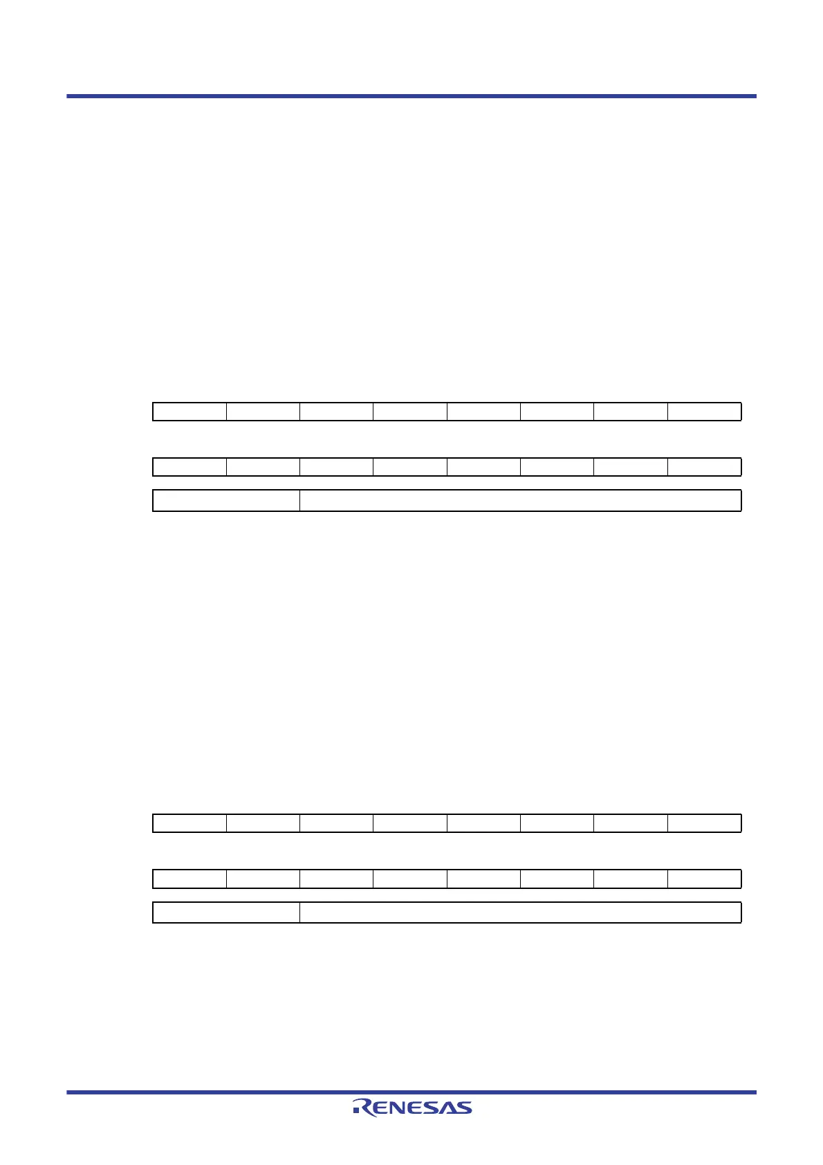
(48) ANTSW output timing setting register (BBANTSWTIMG)
This register is used to set the timing for the ANTSW pin output.
The time to set the ANTSW pin output to high level can be set after the setting of “1” to the transmission
trigger bit.
The value ranged from 001H to 154H can be set while the initial value is 072H (The set value is 1H =
approx.1 μs).
Do not set the values other than those ranged from 001H (Approx. 1 μs) to 154H (Approx.340 μs).
The BBANTSWTIMG register is set by the serial interface in 8-bit units.
Reset signal generation sets this register to 0072H.
Figure 18 - 61 ANTSW Output Timing Setting Register (BBANTSWTIMG) Format
Caution Be sure to clear bits 10 to 15 to “0”.
(49) Receive frame length register (BBRXFLEN)
This register is used to store the frame length value upon reception. The value is stores at the timing when
the packet data reception is started. The value is retained until the start of the next packet data reception.
However, the register is updated when the address match is recognized when the address filter is enabled.
The reading value is corresponding save bank specified by receive data save bank select bit.
The BBRXFLEN register is read by the serial interface in 8-bit units.
Reset signal generation clears this register to 0000H.
Figure 18 - 62 Receive Frame Length Register (BBRXFLEN) Format
Caution “0” is always read for bits 11 to 15.
Address:
007BH, 007AH
After reset:
0072H
R/W
Symbol 15 14 13 12 11 10 9 8
BBANTS
WTIMG
000000
76543210
BBANTSWTIMG Time till the ANTSW pin output is set to high level
Address:
00A1H, 00A0H
After reset:
0000H
R
Symbol 15 14 13 12 11 10 9 8
BBRXFLEN
0 0 0 0 0 RCVFLEN10 RCVFLEN9 RCVFLEN8
76543210
RCVFLEN7 RCVFLEN6 RCVFLEN5 RCVFLEN4 RCVFLEN3 RCVFLEN2 RCVFLEN1 RCVFLEN0
RCVFLEN[10:0] The frame length value upon receive
 Loading...


