RL78/G1H CHAPTER 3 PIN FUNCTIONS
R01UH0575EJ0120 Rev. 1.20 Page 35 of 920
Dec 22, 2016
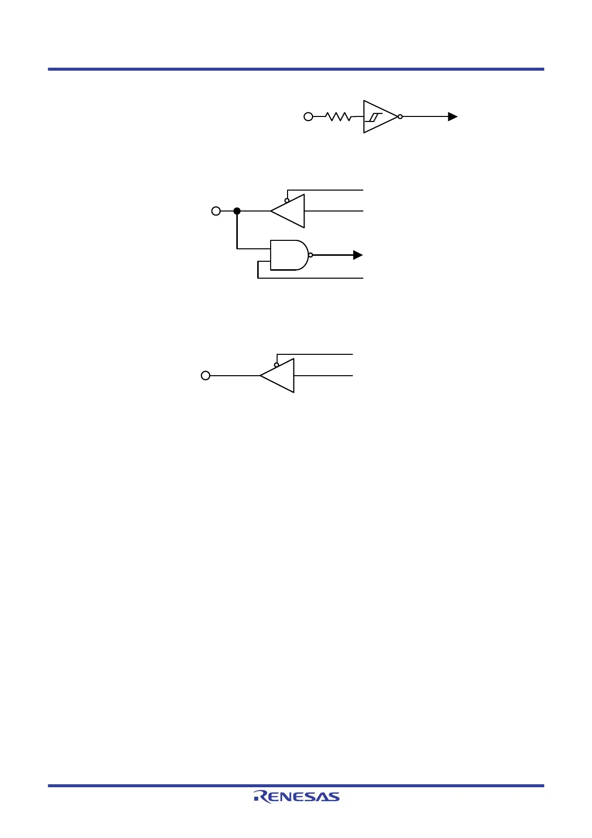
Figure 3 - 14 Pin Block Diagram of STANDBY, MODE1, MODE2
Figure 3 - 15 Pin Block Diagram of Pin GPIO0 to GPIO4
Figure 3 - 16 Pin Block Diagram of Pin INTOUT
STANDBY, MODE1, MODE2 Input
Input enable
GPIO0 to GPIO4
Output enable
Data
Input
INTOUT
Output enable
Data
 Loading...


