RL78/G1H CHAPTER 21 RESET FUNCTION
R01UH0575EJ0120 Rev. 1.20 Page 750 of 920
Dec 22, 2016
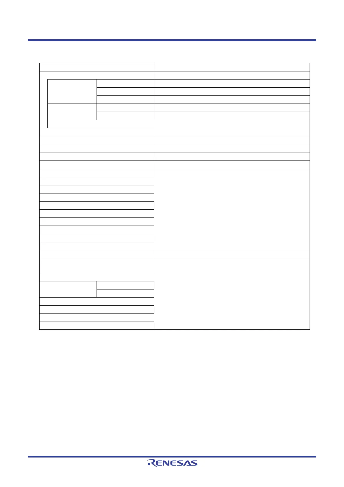
Note P40 and P130 become the following state.
• P40: High-impedance during the external reset period or reset period by the POR. High level during other types of reset
(connected to the on-chip pull-up resistance).
• P130: Low level during the reset period
Remark f
IH: High-speed on-chip oscillator clock fX: X1 oscillation clock
f
EX: External main system clock fXT: XT1 oscillation clock
f
EXS: External subsystem clock fIL: Low-speed on-chip oscillator clock
Table 21 - 1 Operation Statuses During Reset Period
Item During Reset Period
System clock Clock supply to the CPU is stopped.
Main system clock f
IH Operation stopped
f
X Operation stopped (the X1 and X2 pins are input port mode)
f
EX Clock input invalid (the pin is input port mode)
Subsystem clock f
XT Operation stopped (the XT1 and XT2 pins are input port mode)
f
EXS Clock input invalid (the pin is input port mode)
f
IL Operation stopped
CPU
Code flash memory Operation stopped
Data flash memory Operation stopped
RAM Operation stopped
Port (latch)
High impedance
Note
Timer array unit Operation stopped
Timer RJ
Real-time clock (RTC)
12-bit Interval timer
Watchdog timer
Clock output/buzzer output
A/D converter
Serial array unit (SAU)
Serial interface (IICA)
Data transfer controller (DTC)
Power-on-reset function Detection operation possible
Voltage detection function Operation is possible in the case of an LVD reset and stopped in the case
of other types of reset.
External interrupt Operation stopped
CRC operation function High-speed CRC
General-purpose CRC
Illegal-memory access detection function
RAM parity error detection function
RAM guard function
SFR guard function
 Loading...


