RL78/G1H CHAPTER 28 ON-CHIP DEBUG FUNCTION
R01UH0575EJ0120 Rev. 1.20 Page 830 of 920
Dec 22, 2016
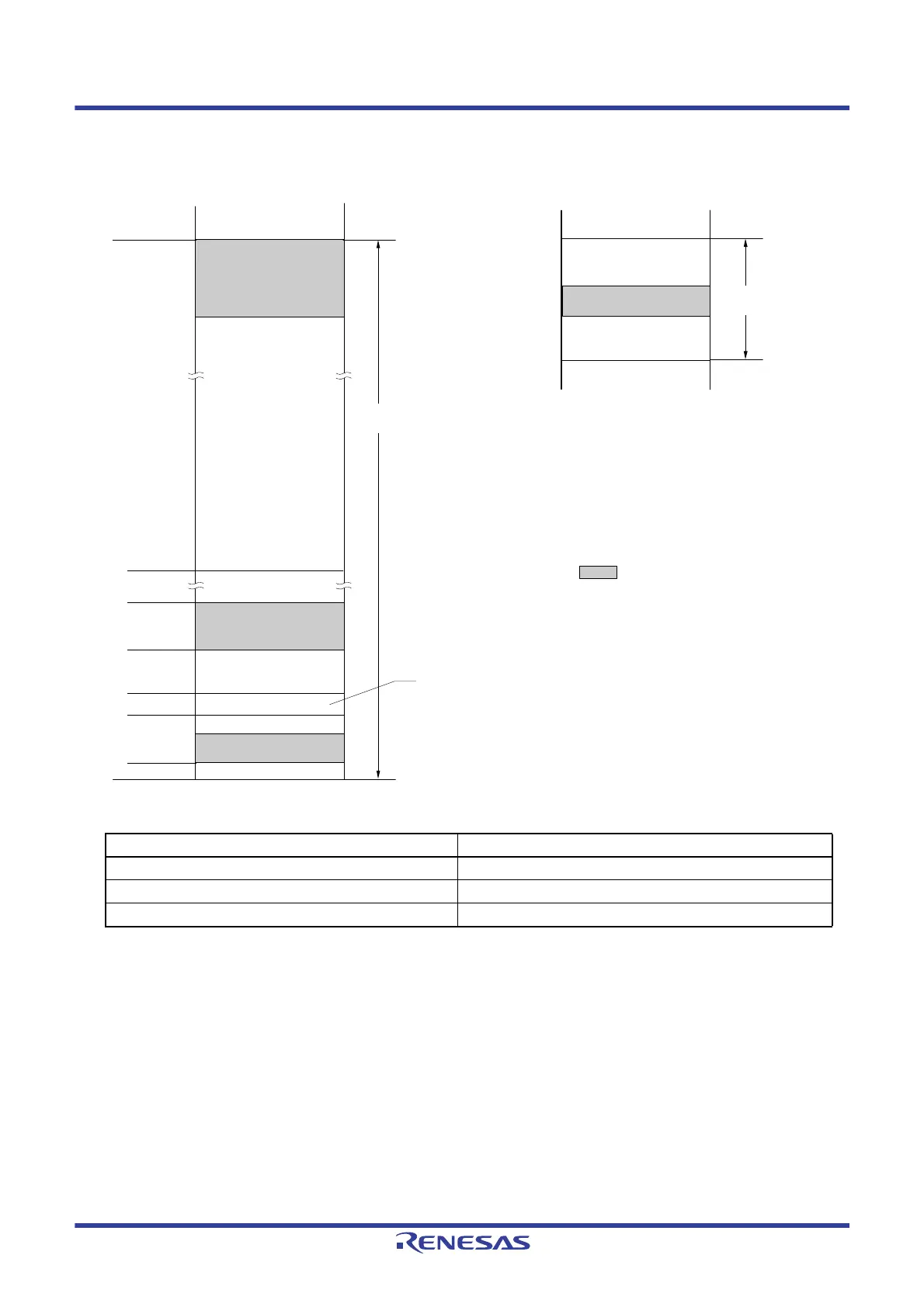
Figure 28 - 2 Memory Spaces Where Debug Monitor Programs Are Allocated
Note 1. Address differs depending on products as follows.
Note 2. When real-time RAM monitor (RRM) function and dynamic memory modification (DMM) function are not used, it is 256
bytes.
Note 3. In debugging, reset vector is rewritten to address allocated to a monitor program.
Note 4. Since this area is allocated immediately before the stack area, the address of this area varies depending on the stack
increase and decrease. That is, 4 extra bytes are consumed for the stack area used.
When using self-programming, 12 extra bytes are consumed for the stack area used.
Products (code flash memory capacity) Address of Note 1.
R5F11FLJ 3FFFFH
R5F11FLK 5FFFFH
R5F11FLL 7FFFFH
Debug monitor area
(10 bytes)
Debug monitor area
(2 bytes)
(512 bytes or
256 bytes
Note 2
)
Note 1
Stack area for debugging
(4 bytes)
Note 4
Internal RAMCode flash memory
Use prohibited
SFR area
Code flash
area
Internal RAM
area
: Area used for on-chip debugging
Mirror area
On-chip debug option byte area
(1 byte)
Security ID area
(10 bytes)
000D8H
000CEH
000C4H
000C3H
00002H
00000H
01000H
Note 3
 Loading...


