xiii
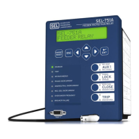
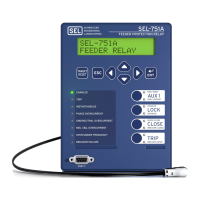
Date Code 20100129 Instruction Manual SEL-751A Relay
List of Figures
Figure 4.43 Schematic Diagram of a Traditional Latching Device......................................................... 4.82
Figure 4.44 Logic Diagram of a Latch Switch ........................................................................................ 4.82
Figure 4.45 SEL
OGIC Control Equation Variable/Timers SV01/SV01T—SV32T ................................. 4.83
Figure 4.46 Result of Falling-Edge Operator on a Deasserting Input ..................................................... 4.86
Figure 4.47 Example Use of SEL
OGIC Variables/Timers ........................................................................ 4.88
Figure 4.48 Counter 01............................................................................................................................ 4.89
Figure 4.49 Example of the Effects of the Input Precedence .................................................................. 4.90
Figure 4.50 Phase Rotation Setting ......................................................................................................... 4.92
Figure 4.51 Breaker Failure Logic........................................................................................................... 4.95
Figure 4.52 Arc-Flash Instantaneous Overcurrent Element Logic .......................................................... 4.96
Figure 4.53 Inverse Time-Overlight Element Logic................................................................................ 4.97
Figure 4.54 TOL Element Inverse Curve Characteristic ......................................................................... 4.98
Figure 4.55 Analog Input Card Adaptive Name.................................................................................... 4.100
Figure 4.56 Settings to Configure Input 1 as a 4–20 mA Transducer ................................................... 4.103
Figure 4.57 Analog Output Number Allocation .................................................................................... 4.104
Figure 4.58 Analog Output Settings ...................................................................................................... 4.105
Figure 4.59 DC Mode Processing.......................................................................................................... 4.106
Figure 4.60 AC Mode Processing.......................................................................................................... 4.106
Figure 4.61 Timing Diagram for Debounce Timer Operation When Operating in AC Mode .............. 4.106
Figure 4.62 Display Point Settings ........................................................................................................ 4.114
Figure 4.63 Front-Panel Display—Both HV and LV Breakers Open ................................................... 4.115
Figure 4.64 Front-Panel Display—HV Breaker Closed, LV Breaker Open.......................................... 4.115
Figure 4.65 Front-Panel Display—Both HV and LV Breakers Closed ................................................. 4.115
Figure 4.66 Front-Panel Display—HV Breaker Open, LV Breaker Closed.......................................... 4.115
Figure 4.67 Front-Panel Display—HV Breaker Open, LV Breaker Closed.......................................... 4.115
Figure 4.68 Front-Panel Display for a Binary Entry in the Name String Only..................................... 4.116
Figure 4.69 Front-Panel Display for an Analog Entry in the Name String Only .................................. 4.116
Figure 4.70 Front-Panel Display for an Entry in (a) Boolean Name and Alias Strings and
(b) Analog Name and User Text and Formatting Strings ............................................... 4.117
Figure 4.71 Front-Panel Display for an Entry in (a) Boolean Name and Alias Strings and
(b) Analog Name, User Text and Formatting Strings, and Engineering Units............... 4.117
Figure 4.72 Adding Temperature Measurement Display Points ........................................................... 4.118
Figure 4.73 Rotating Display................................................................................................................. 4.119
Figure 4.74 Adding Two Local Bits ...................................................................................................... 4.120
Figure 5.1 Complex Power Measurement Conventions .......................................................................... 5.2
Figure 5.2 METER Command Report With Enhanced Voltage Option With Monitoring Package........ 5.4
Figure 5.3 METER T Command Report With RTDs .............................................................................. 5.5
Figure 5.4 Device Response to the METER E Command....................................................................... 5.5
Figure 5.5 Device Response to the METER RE Command.................................................................... 5.6
Figure 5.6 Device Response to the METER M Command...................................................................... 5.7
Figure 5.7 Device Response to the METER RM Command................................................................... 5.7
Figure 5.8 Device Response to the METER MV Command................................................................... 5.7
Figure 5.9 Device Response to the METER RMS Command................................................................. 5.8
Figure 5.10 Device Response to the METER AI Command..................................................................... 5.8
Figure 5.11 Device Response to the METER L (Light) Command .......................................................... 5.9
Figure 5.12 Device Response to the MET DE Command......................................................................... 5.9
Figure 5.13 Device Response to the MET PE Command........................................................................ 5.10
Figure 5.14 Device Response to the LDP Command .............................................................................. 5.11
Figure 5.15 DC Under- and Overvoltage Elements................................................................................. 5.12
Figure 5.16 Create DC Voltage Elements With SEL
OGIC Control Equations......................................... 5.13
Figure 5.17 Plotted Breaker Maintenance Points for a 25 kV Circuit Breaker ....................................... 5.17
Figure 5.18 SEL-751A Breaker Maintenance Curve for a 25 kV Circuit Breaker ................................. 5.18
Figure 5.19 Operation of SEL
OGIC Control Equation Breaker Monitor Initiation Setting ..................... 5.19
Figure 5.20 Breaker Monitor Accumulates 10 Percent Wear.................................................................. 5.20
Figure 5.21 Breaker Monitor Accumulates 25 Percent Wear.................................................................. 5.21
Figure 5.22 Breaker Monitor Accumulates 50 Percent Wear.................................................................. 5.22
Figure 5.23 Breaker Monitor Accumulates 100 Percent Wear................................................................ 5.23
Figure 5.24 Input INxxx Connected to Trip Bus for Breaker Monitor Initiation .................................... 5.25