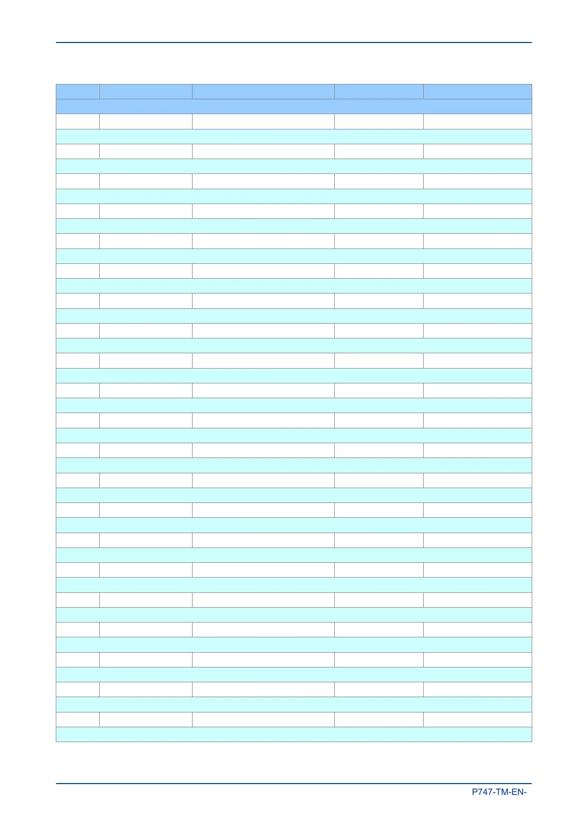
Ordinal Signal Name Source Type Response
Description
205 I>3 Timer Block Programmable Scheme Logic PSL Output No response
This DDB signal blocks the third stage overcurrent time delay
206 I>4 Timer Block Programmable Scheme Logic PSL Output No response
This DDB signal blocks the fourth stage overcurrent time delay
243 I>1 Trip Software PSL Input Protection event
This DDB signal is the first stage any-phase Phase Overcurrent trip signal
244 I>1 Trip A Software PSL Input Protection event
This DDB signal is the first stage A-phase Phase Overcurrent trip signal
245 I>1 Trip B Software PSL Input Protection event
This DDB signal is the first stage B-phase Phase Overcurrent trip signal
246 I>1 Trip C Software PSL Input Protection event
This DDB signal is the first stage C-phase Phase Overcurrent trip signal
247 I>2 Trip Software PSL Input Protection event
This DDB signal is the second stage any-phase Phase Overcurrent trip signal
248 I>2 Trip A Software PSL Input Protection event
This DDB signal is the second stage A-phase Phase Overcurrent trip signal
249 I>2 Trip B Software PSL Input Protection event
This DDB signal is the second stage B-phase Phase Overcurrent trip signal
250 I>2 Trip C Software PSL Input Protection event
This DDB signal is the second stage C-phase Phase Overcurrent trip signal
251 I>3 Trip Software PSL Input Protection event
This DDB signal is the third stage any-phase Phase Overcurrent trip signal
252 I>3 Trip A Software PSL Input Protection event
This DDB signal is the third stage A-phase Phase Overcurrent trip signal
253 I>3 Trip B Software PSL Input Protection event
This DDB signal is the third stage B-phase Phase Overcurrent trip signal
254 I>3 Trip C Software PSL Input Protection event
This DDB signal is the third stage C-phase Phase Overcurrent trip signal
255 I>4 Trip Software PSL Input Protection event
This DDB signal is the fourth stage any-phase Phase Overcurrent trip signal
256 I>4 Trip A Software PSL Input Protection event
This DDB signal is the fourth stage A-phase Phase Overcurrent trip signal
257 I>4 Trip B Software PSL Input Protection event
This DDB signal is the fourth stage B-phase Phase Overcurrent trip signal
258 I>4 Trip C Software PSL Input Protection event
This DDB signal is the fourth stage C-phase Phase Overcurrent trip signal
295 I>1 Start Software PSL Input Protection event
This DDB signal is the first stage any-phase Overcurrent start signal
296 I>1 Start A Software PSL Input Protection event
This DDB signal is the first stage A-phase Overcurrent start signal
297 I>1 Start B Software PSL Input Protection event
This DDB signal is the first stage B-phase Overcurrent start signal
Chapter 5 - Protection Functions MiCOM P747
134 P747-TM-EN-1

 Loading...