4.8 CIRCUIT BREAKER MAPPING
CB Closed 3 ph CB in Service
V02026
Key: External DDB Signal
Figure 87: Circuit Breaker mapping
4.9 FAULT RECORD TRIGGER MAPPING
Output R3 Fault Rec Trig
V02027
Key: External DDB Signal
Figure 88: Fault Record Trigger mapping
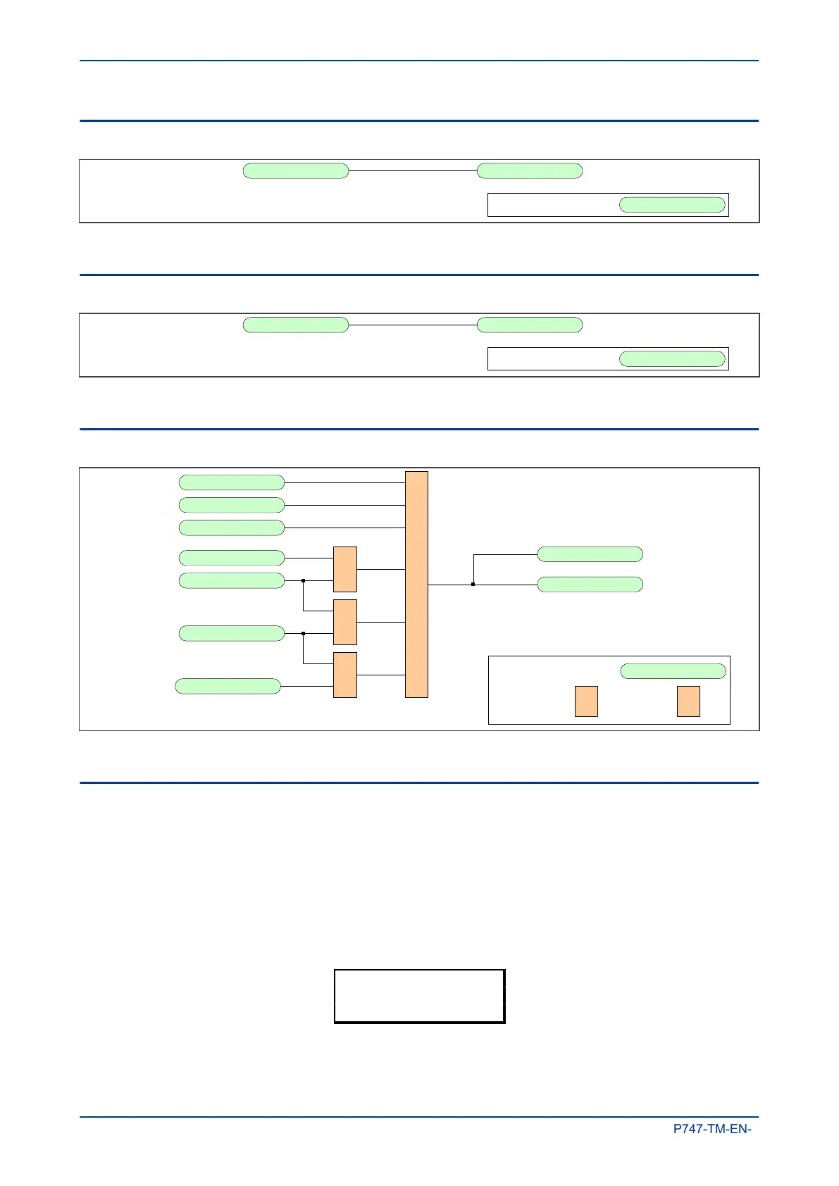
4.10 CHECK SYNCHRONISATION AND VOLTAGE MONITOR MAPPINGS
SysChks Inactive
V
02028
Key: External DDB Signal
O
R gate
1 &AND gate
Man Check Synch
AR Sys Checks
Check Sync 1 OK
Check Sync 2 OK
Live Line
Dead Bus
Dead Line
Live Bus
1
&
&
&
Figure 89: Check Synchronisation and Voltage Monitor mappings
4.11 SETTINGS
The device contains a PSL DATA column, which can be used to track PSL modifications. A total of 12 cells
are contained in the PSL DATA column; 3 for each setting group.
Grp(n) PSL Ref: When downloading a PSL scheme to an IED, you will be prompted to enter the relevant
group number and a reference identifier. The first 32 characters of the reference identifier are displayed in
this cell. The horizontal cursor keys can scroll through the 32 characters as the LCD display only displays 16
characters.
Example:
Grp. PSL Ref.
Date/time: This cell displays the date and time when the PSL scheme was downloaded to the IED.
Example:
Chapter 12 - Scheme Logic MiCOM P747
326 P747-TM-EN-1
 Loading...