I/O Controller Hub
128 Design Guide
NOTES:
1. The SMBus device must be back-drive safe while its supply (VCC_3.3) is off and 3.3 V SUS is still powered.
2. In suspended modes where VCC_3.3 is OFF and 3.3 V SUS is on, the VCC_3.3 node will be very near
ground. In this case, the input leakage of the ICH3-S will be approximately 10 µA.
9.6 Real Time Clock (RTC)
The ICH3-S contains a real time clock (RTC) with 256 bytes of battery-backed SRAM. The
internal RTC module provides two key functions: keeping date and time, and storing system data in
its RAM when the system is powered down.
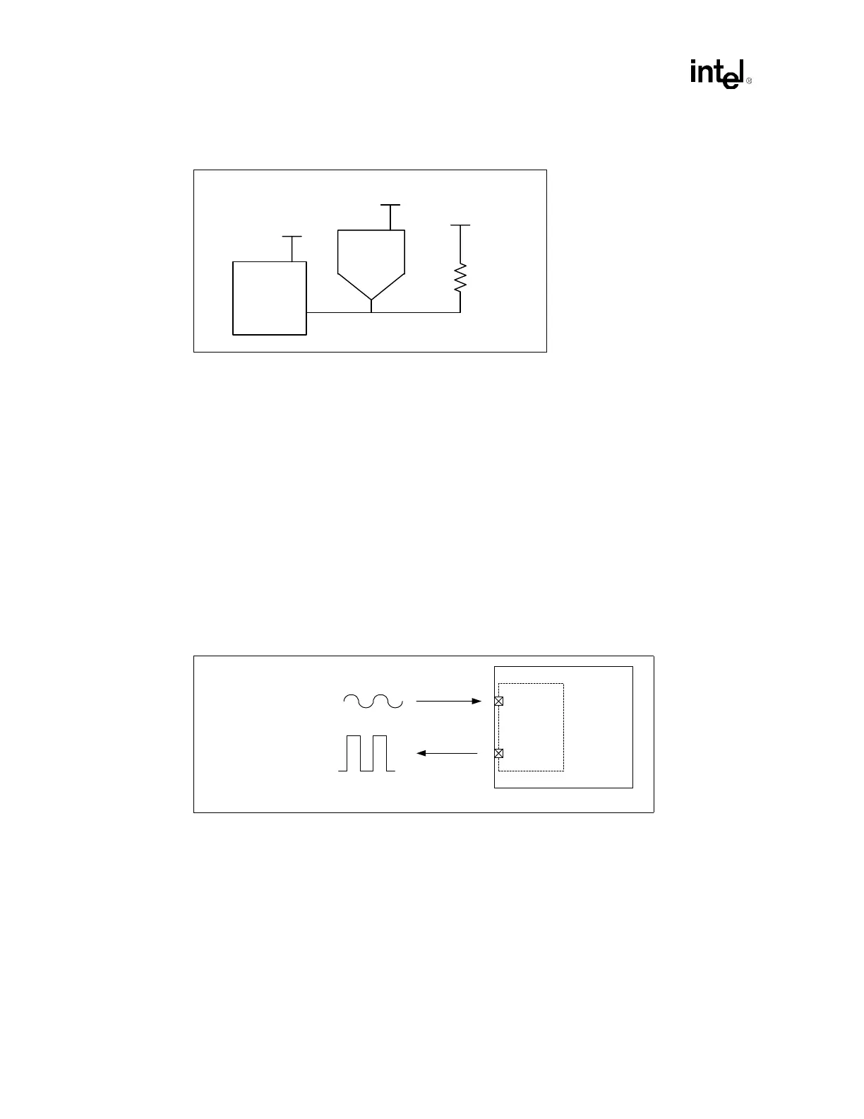
The ICH3-S uses a crystal circuit that generates a low-swing 32 kHz input sine wave. The RTCX1
input is amplified and driven back to the crystal circuit via the RTCX2 signal. Internal to the
ICH3-S, the RTCX1 signal is amplified to drive internal logic as well as generate a free running
full swing clock output for system use illustrated in Figure 9-9. This ICH-S output ball is called
SUSCLK.
For further information on the RTC, consult Intel application note AP-728 Intel
®
ICH Family Real
Time Clock (RTC) Accuracy and Considerations Under Test Conditions (http://
developer.intel.com/design/chipsets/applnots/292276.htm).
This section presents the recommended hookup for the RTC circuit for the ICH3-S.
Figure 9-8. Unified VCC_3.3 Architecture
Intel
®
ICH3-S
3.3 VSUS
SMBus
Devices
VCC_3.3
VCC_3.3
SMBus
8.2 k
Ω
Figure 9-9. RTCX1 and SUSCLK Relationship
Intel
®
ICH3-S
Internal
Oscillator
RTCX1
SUSCLK
Low-Swing 32.768kHz
Sine Wave Source
Full-Swing 32.768kHz
Output Signal