Platform Clock Routing Guidelines
38 Design Guide
4.1 Clock Groups
4.1.1 HOST_CLK Clock Group
4.1.1.1 HOST_CLK Clock Topology
The clock synthesizer provides four sets of 100 MHz differential clock outputs. The 100 MHz
differential clocks are driven to the Processors, the MCH, and the processors’ debug port as shown
in Figure 4-1.
The clock driver differential bus output structure is a “Current Mode Current Steering” output
which develops a clock signal by alternately steering a programmable constant current to the
external termination resistors “Rt.” The resulting amplitude is determined by multiplying IOUT by
the value of Rt. The current IOUT is programmable by a resistor and an internal multiplication
factor so the amplitude of the clock signal can be adjusted for different values of “R”’ to match
impedances or to accommodate future load requirements.
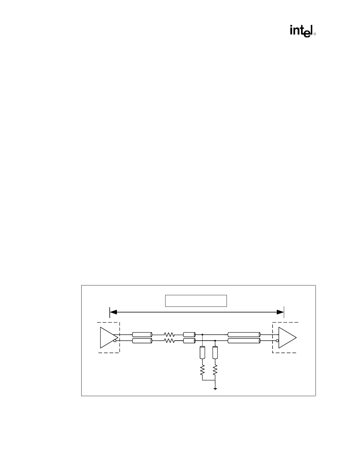
The recommended termination for the differential bus clock is a “Shunt Source Termination.”
Refer to Figure 4-2 for an illustration of this termination scheme. Parallel Rt resistors perform a
dual function, converting the current output of the clock driver to a voltage and matching the driver
output impedance to the transmission line. The series resistors “Rs” provide isolation from the
clock driver's output parasitics, which would otherwise appear in parallel with the termination
resistor Rt.
The value of Rt should be selected to match the characteristic impedance of the motherboard, and
Rs should be between 20 Ω and 33 Ω. Simulations have shown that Rs values above 33 Ω provide
no benefit to signal integrity but only degrade the edge rate.
• Mult0 pin (pin #43) is pulled high – making the multiplication factor 6.
• Iref pin (pin # 42) is connected to ground through a 475 Ω ± 1% resistor – making the Iref
2.32 mA.
Figure 4-2. Source Shunt Termination
L1'
L1
Rs
L2
L2'
L3 L3'
L4
L4'
Clock
Driver
Processor or
MCH
Rs
Rt Rt
LT = L1 + L2 + L4