Design Guide 181
Platform Power Delivery Guidelines
12.4 Intel
®
ICH3-S Power Delivery Guidelines
12.4.1 1.8 V/3.3 V Power Sequencing
The ICH3-S has two pairs of associated 1.8 V and 3.3 V supplies. These are {VCC_1.8, VCC_3.3}
and {VCCSUS_1.8, VCCSUS_3.3}. The difference between the two associated supplies must
never be greater than 2.0 V. The 1.8 V supply may come up before the 3.3 V supply without
violating this rule (though this generally does not occur because the 1.8 V supply is typically
derived from the 3.3 V supply with a linear regulator). One serious consequence of violation of this
“2 V Rule” is electrical overstress of oxide layers, resulting in component damage.
The majority of the ICH3-S I/O buffers are driven by the 3.3 V supplies but are controlled by logic
powered by the 1.8 V supplies. Therefore, another consequence of faulty power sequencing arises
if the 3.3 V supply comes up first. In this case, the I/O buffers will be in an undefined state until the
1.8 V logic is powered up. Some signals that are defined as “Input-only” actually have output
buffers that are normally disabled, and the ICH3-S may unexpectedly drive these signals if the
3.3 V supply is active while the 1.8 V supply is not.
Figure 12-21 is an example of power-on sequencing circuit that ensures the 2 V Rule is obeyed.
This circuit uses an NPN (Q2) and a PNP (Q1) transistor to ensure the 1.8 V supply tracks the 3.3
V supply. The NPN transistor controls the current through PNP from the 3.3 V supply into the 1.8
V power plane by varying the voltage at the base of the PNP transistor. By connecting the emitter
of the NPN transistor to the 1.8 V plane, current will not flow from the 3.3 V supply into 1.8 V
plane when the 1.8 V plane reaches 1.8 V.
Note: Note that such circuit is not needed if the voltage regulator guarantees the 2 V Rule.
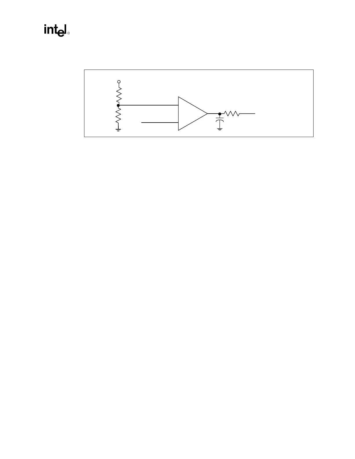
Figure 12-20. Sample 2.5 V Output Enable Control Logic
+
–
420 Ω
240 Ω
VCC_3.3
VCC_1.2
2.5V_OUTPUT
_ENABLE
10 k Ω
0.1 µF