System Bus Routing Guidelines
58 Design Guide
Therefore, the PCB trace length of DSTB0 must be within ±25 mils of 4.356" from Processor 0 to
Processor 1.
Calculate CPU to MCH length assuming the CPU to MCH PCB length to be 9.0":
CPU
pin
-to-MCH
pin
(HD4) (motherboard trace from Processor 0 to Processor1) = 9.000"
MCH
pkg_len
(DSTBP0) (strobe package trace length) = 0.190"
MCH
pkg_len
(HD4) (HD4 package trace length) = 0.280"
CPU1
pkg_comp
(DSTBP0) = 0.78 * CPU
pkg_len
(DSTBP0) = 0.78 * 0.150" = 0.117"
CPU1
pkg_comp
(HD4) = 0.78 * CPU1
pkg_len
(HD4) = 0.78 * 0.350" = 0.273"
CPU
pin
-to-MCH
pin
(DSTBP0) = MCH
pkg_len
(HD4) + CPU
pin
-to-MCH
pin
(HD4)
+ CPU1
pkg_comp
(HD4) – MCH
pkg_len
(DSTBP0) – CPU1
pkg_comp
(DSTBP0)
= 0.280 + 9.000 + 0.273 – 0.190 – 0.117
CPU
pin
-to-MCH
pin
(DSTBP0) = 9.246"
Therefore, the PCB trace length of DSTB0 must be within ± 25 mils of 9.246" from Processor 1
to the MCH.
5.2 Routing Guidelines for Common Clock Signals
Table 5-5 lists the Common clock signals.
Route the common clock signals according to the processor system bus topology shown in
Figure 5-1. Routing guidelines for the common clock signal group are in Table 5-2. Route the
traces with at least 50% of the trace width directly over a reference plane.
5.2.1 Wired-OR Signals
There are five “wired-OR” signals on the system bus. These signals are HIT#, HITM#, MCERR#,
BINIT#, and BNR#. These signals differ from the other system bus signals in that more than one
agent can be driving the signal at the same time. However, Intel recommends that special attention
be given to the routing of these signals in adherence to the layout guidelines presented in Table 5-2.
Timing and signal integrity must be met for the cases where one agent is driving, all agents are
driving, and any combination of agents are driving.
The wired-OR signals should follow the same routing rules as the common clock signals. Intel
recommends that simulations for these signals be performed for each system.
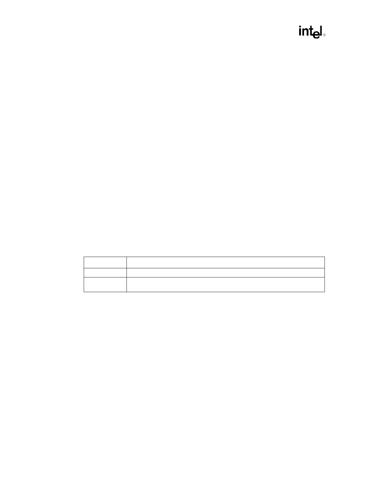
Table 5-5. AGTL+ Common Clock I/O Signals
Signal Types Signals
Input BPRI#, BR[3:1]#, DEFER#, RESET#, RS[2:0]#, RSP#, TRDY#
I/O
ADS#, AP[1:0]#, BINIT#, BNR#, BPM[5:0]#, BR0#, DBSY#, DP[3:0]#, DRDY#, HIT#,
HITM#, LOCK#, MCERR#