Design Guide 39
Platform Clock Routing Guidelines
NOTES:
1. The skew budget includes clock driver output pair to output pair jitter (differential jitter) and skew, clock skew
due to interconnect process variation, and static skew due to layout differences between clocks to all bus
agents.
2. This number does not include clock driver common mode (cycle to cycle) jitter or spread spectrum clocking.
3. The interconnect portion of the total budget for this specification assumes clock pairs are routed on multiple
routing layers and routed no longer than the maximum recommended lengths.
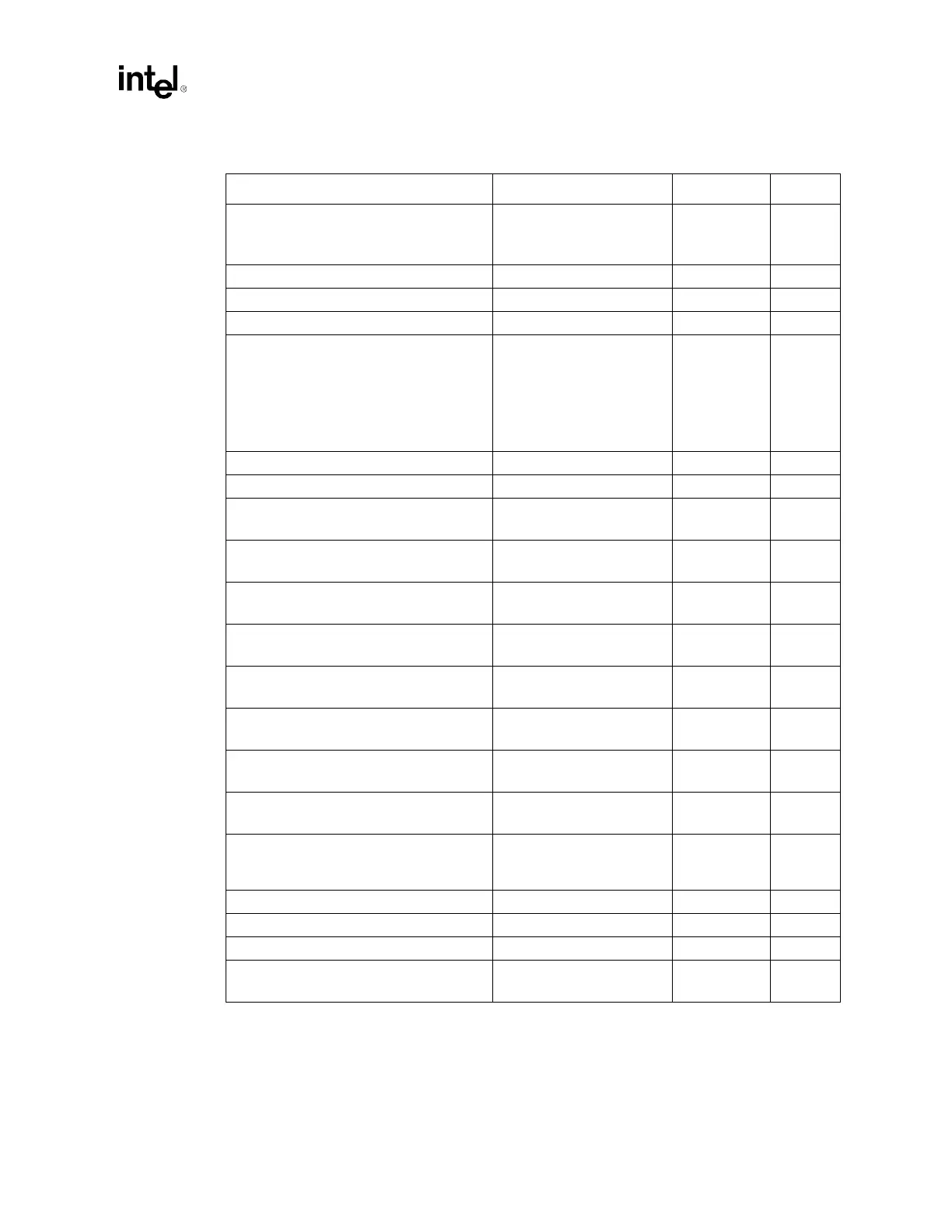
Table 4-3. HOST_CLK[1:0]# Routing Guidelines
Layout Guideline Value Illustration Notes
HOST_CLK Skew between Agents
300 ps total budget:
150 ps for clock driver
150 ps for interconnect
Figure 4-2
and
Figure 4-3
1,2,3,4
Trace Width 5 mils Figure 4-4
Differential Pair Spacing 20 – 25 mils Figure 4-4 5,6
Spacing to Other Traces 25 mils Figure 4-4
Serpentine Spacing
Maintain a minimum S/h ratio
of > 5/26
Keep parallel serpentine
sections as short as possible.
Minimize 90 degree bends.
Make 45 degree bends, if
possible.
Figure 4-4
Motherboard Impedance – Differential 100
Ω typical 8
Motherboard Impedance – Single Ended 50
Ω ± 10% 9
Processor Routing Length –
L1, L1’: Clock Driver to Rs
0 – 0.5” Figure 4-2 13
Processor Routing Length –
L2, L2’: Rs to Rs-Rt Node
0 – 0.2” Figure 4-2 13
Processor Routing Length –
L3, L3’: Rs-Rt Node to Rt
0 – 0.2” Figure 4-2 13
Processor Routing Length –
L4, L4’: Rs-Rt Node to Load
0 – 22” Figure 4-2
MCH Routing Length –
L1, L1’: Clock Driver to Rs
0 – 0.5” Figure 4-2 13
MCH Routing Length –
L2, L2’: Rs to Rs-Rt Node
0 – 0.2” Figure 4-2 13
MCH Routing Length –
L3, L3’: Rs-Rt Node to Rt
0 – 0.2” Figure 4-2 13
MCH Routing Length –
L4, L4’: Rs-Rt Node to Load
0 – 22” Figure 4-2
Processor to MCH Length Matching (LT)
0.035” ± 0.010”
MCH LT must be 0.076”
longer than Processor LT.
Figure 4-2 10
Processor to Processor Length Matching (LT)
± 10 mils Figure 4-2 15
HOST_CLK0 – HOST_CLK1 Length Matching ± 10 mils
Rs Series Termination Value 20 – 33
Ω ± 5% Figure 4-2 11
Rt Shunt Termination Value
49.9
Ω ± 1%
(for 50
Ω board impedance)
Figure 4-2 12