Platform Stack-Up and Component Placement Overview
32 Design Guide
3.2 Platform Stack-Up
Figure 3-2 shows the recommended platform stack-up. All layers are 1 oz copper. The processor
requires 2 oz of copper to deliver power and 2 oz of copper to deliver ground. Vias are 10 mil
finished hole with 35 mil anti-pads and 24 mil pads.
Route signal layers as asymmetric stripline on layers 2, 4, 5 and 7. The signal layers must reference
ground on layer 3 or layer 6 only. Route signals on layers 4 and 5 orthogonally to reduce crosstalk
between the layers.
Intel strongly recommends that system designers use the stack-up shown in Figure 3-2 and
recommendations in Table 3-2 when designing their boards. Intel realizes numerous ways exist to
achieve these targeted impedance tolerances; contact your board vendor for these specifics. Intel
encourages platform designers to perform comprehensive simulation analysis to ensure all timing
specifications are met. This is particularly important if a design deviates from the design guidelines
provided.
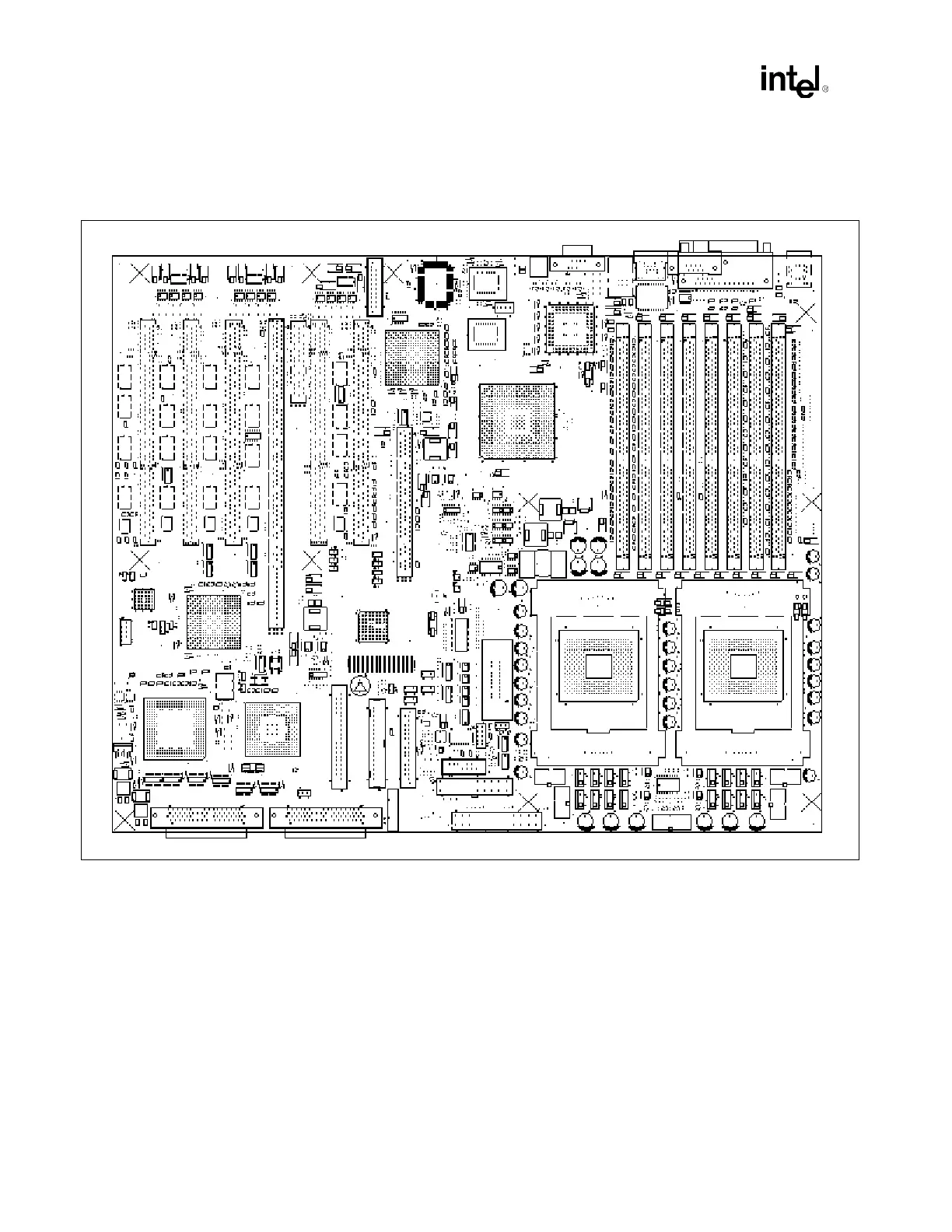
Figure 3-1. Intel
®
E7500 Chipset Customer Reference Board System Placement Example