Design Guide 55
System Bus Routing Guidelines
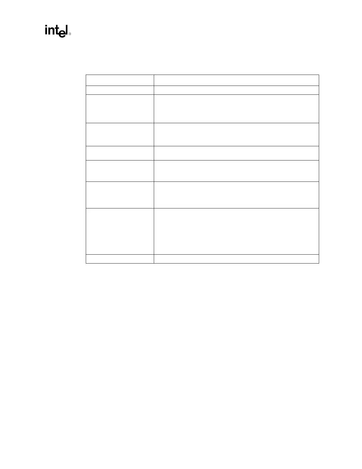
Table 5-2. System Bus Routing Summary
Parameter Platform Routing Guidelines
Trace Width/Spacing 5/15 mils.
2X and 4X Signal Group Line
Lengths
(Agent-to-Agent Length)
3.0" – 10.1" pin-to-pin.
Total bus length must not exceed 20.2".
Trace lengths must be balanced ± 25 mils with respect to the strobe between
agents to compensate for the stub created by the processor package.
DSTBN3[:0]# / DSTBP[3:0]#
and ADSTB[1:0]# Line
Lengths
Should follow the same routing rules as the 2X and 4X Signal Group.
A 25 mil spacing should be maintained around each strobe signal.
Do not route differentially.
Common Clock Signal Line
Lengths
Common Clock signals should follow the same routing rules as the Data
signals, however no length compensation is necessary.
Topology Daisy chain with the chipset at one end of the system bus and Processor 0 at
the other.
End processor must have on-die termination enabled.
Routing Requirements No motherboard contribution to stub length of middle processor (< 35 mil
trace from via to pad).
All signals within the same strobe group must be routed on same layer for
entire length of bus.
Reference Plane
Requirements
Ground referenced only.
Avoid changing layers when routing system bus signals.
If a layer change must occur, use vias connecting the two reference planes to
provide a low impedance path for the return current. Vias should be as close
as possible to the signal via.
For 2X and 4X signals, ADSTB[1:0]#, and DSTBN3[:0]# / DSTBP[3:0]#:
NEVER ROUTE OVER A PLANE SPLIT.
Motherboard Impedance 50
Ω ± 10%.