Design Guide 179
Platform Power Delivery Guidelines
12.3.5 Filter Specifications (1.2V Power Plane)
VCCA_1.2 and VCCAHI_1.2 are created by using a low pass filter on VCC_1.2. VCCACPU is
created by using a low pass filter on VCC_CPU. The MCH has internal analog PLL clock
generators, which require quiet power supplies for minimum jitter. Jitter is detrimental to a system;
it degrades external I/O timings, as well as internal core timings (i.e., maximum frequency).
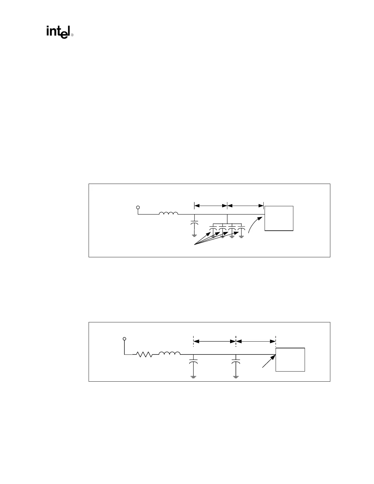
When designing the VCCA_1.2 filter (Figure 12-16), follow these guidelines:
• One 54 nH Inductor close to the edge of the package (within 1" of the die).
• One 100 µF or 150 µF LF capacitor close to the edge of the package.
• Minimum of two (four preferred) Low ESL HF capacitors, 0.22 µF or 0.1 µF, on the backside
of the motherboard under the die.
• Route the VCCA_1.2 trace 1 inch, 35 mils wide with 15 mils spacing on three signal layers of
the motherboard; connect to VCCA_1.2 island on signal layers directly under the MCH core.
When designing the VCCA_1.2 and VCCACPU filters (Figure 12-17 and Figure 12-18), follow
these guidelines:
• One 100 nH Inductor close to the edge of the package (within 1 inch of the die).
• One 100 µF or 150 µF LF capacitor close to the edge of the package.
• Minimum of one Low ESL HF capacitor, 0.1 µF on the motherboard backside, under the die.
Figure 12-16. Filter Topology for VCCA_1.2 (DDR Interface)
VCC_1.2
VCCA_1.2
54 nH
MCH
Within 1"
of Ball
RC Network
Within 1"
100 µF
Route to Balls P20,
T20, V20, Y20,
Y18, Y16, Y14
0.1 µF
Figure 12-17. Filter Topology for VCCAHI_1.2 (HUB Interface)
VCC_1.2
100 nH
1 Ω
VCCAHI_1.2
100 µF
0.1 µF
MCH
RLC Network
Within 1"
Within 1"
of Ball
Route to
ball P16