System Bus Routing Guidelines
64 Design Guide
The SM_TS_A[1:0] signals set the SMBus address for the thermal device on the processor. These
signals must be set at power up with a unique address per bus. The SM_TS_A[1:0] can be set to
logic high, logic low, or a high impedance state giving nine possible combinations of addresses.
Refer to the section on SMBus Device Addressing in the Processor datasheet for addressing details.
The SM_TS_A[1:0] signals do not have an internal pull-down and thus must be pulled to VSS or
SM_VCC with a 1 kΩ ± 5% or smaller resistor. Leaving the pins floating achieves a high-Z state.
The SM_WP signal is a write protect signal for the memory device. Pulling this signal to SM_VCC
with a 100 Ω ± 5% resistor enables write protection. SM_WP has an internal 10 kΩ pull-down.
5.3.5 System Bus COMP Routing Guidelines
Terminate the processor COMP[1:0] pins to ground through 50 Ω ± 1% resistors. Do not wire the
COMP pins together—connect each pin to its own termination resistor.
Terminate the MCH HXRCOMP and HYRCOMP with a 25 Ω ± 1% resistor pull-down to ground.
Terminate the MCH HXSWING and HYSWING using a 150 Ω ± 1% resistor pull-down to ground,
and a 301 Ω ± 1% pull-up to VCC_CPU, respectively. Use two 0.01 µF decoupling capacitors.
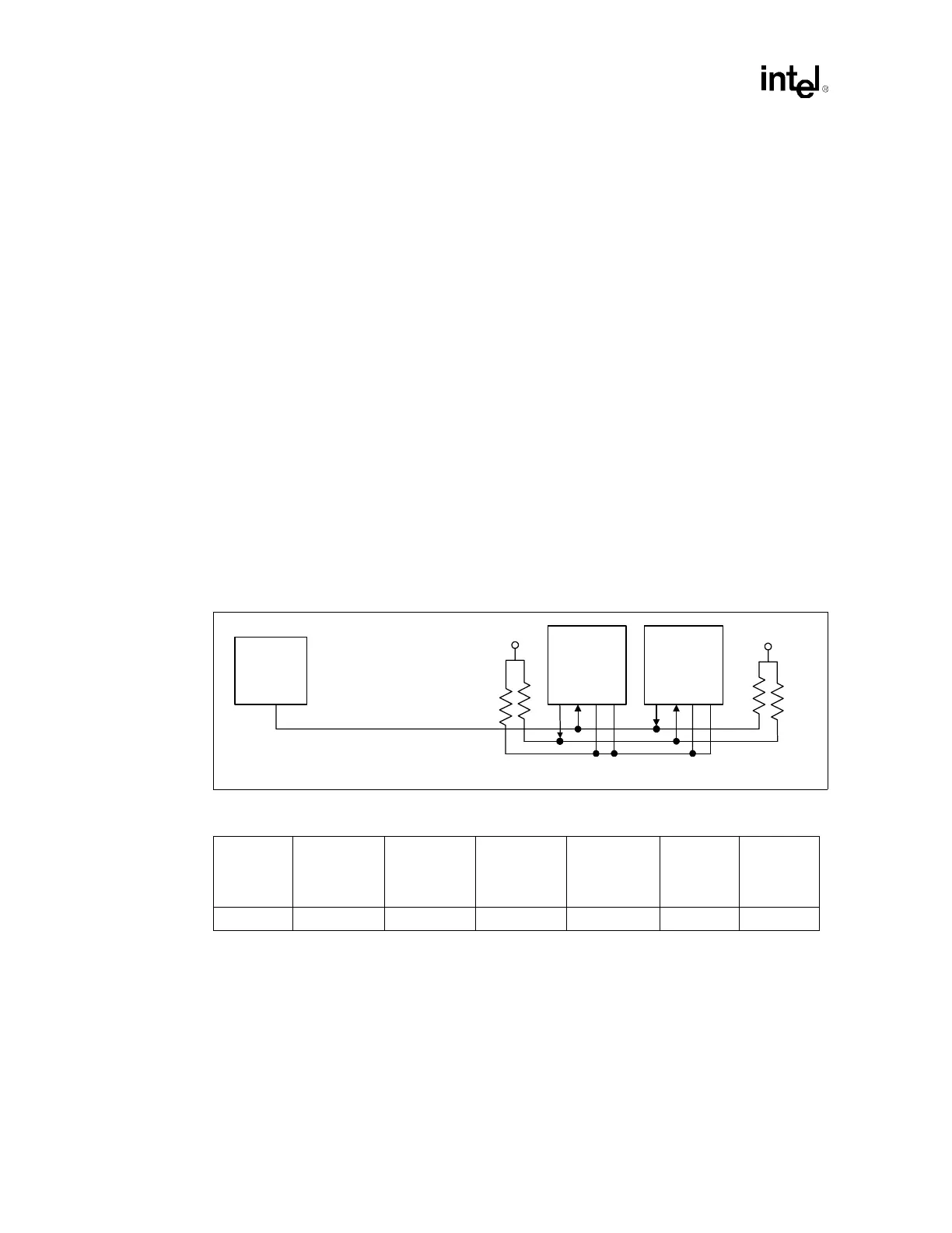
5.3.6 BR[3:0]# Routing Guidelines
Connect BR[3:0]# as shown in Figure 5-10. The total bus length must be less than 20.2". BR3# and
BR2# are not used and are pulled to VCC_CPU.
5.3.7 ODTEN Signal Routing Guidelines
Processor 0, the end processor in a dual processor system, must have its on-die termination
enabled. The termination value must be within 20% of the signal impedance (50 Ω ± 20%). To
enable the on-die termination, pull the ODTEN pin to a high state by terminating it to VCC_CPU
through a 50 Ω ± 20% resistor. Processor 1, the middle agent, must have its on-die termination
disabled. To disable on-die termination, pull the ODTEN pin to a low state by terminating it to
ground through a 50 Ω ± 20% resistor.
Figure 5-10. BR[3:0]# Connection for DP Configuration
Table 5-7. BR[3:0]# Connection
Trace
Impedance
L1
Processor-
to-Processor
L2
Processor1
BR1# to
Intel
®
MCH
L3
Processor-
to-R
T
Stub
L4
Processor-to-
R
PU
Stub
R
T
R
PU
50 Ω 3.0 – 10.0” 15.7” max 1” max 3” max 50 Ω ± 5% 50 Ω ± 5%
MCH
Processor 1
BR0#
BR1#
BR2#
BR3#
BR0#
BR1#
BR2#
BR3#
VCC_CPU
Rpu
Processor 0
L1
L2
L4
VCC_CPU
BREQ0#
R
T
RT
RT
L3
L3
L3