Design Guide 169
Platform Power Delivery Guidelines
12.2.7 Voltage Sequencing
When designing a system with multiple voltages, there is always the issue of ensuring that no
damage occurs to the system during voltage sequencing. Voltage sequencing is the timing
relationship between two or more voltages such as VCC_CPU and SM_VCC.
SM_VCC is required for correct operation of the Intel Xeon processor VID logic.The Intel Xeon
processor’s VID outputs use an active driver. A 3.3 V source connected to the processor’s
SM_VCC pins supplies the VID output devices. As shown in Figure 12-7, the VID outputs will be
valid within 10 ms after the 3.3 V supply reaches 95% of its nominal value. The system power
supply should generate PWR_OK no less than 100 ms after all of its outputs reach their respective
95% values. PWR_OK may be used to enable the VR output. For example a supply adhering to
ATX12V design guidelines meets this requirement. The VR’s PWRGD output may be used to
generate the PWRGOOD input to the processor. PWR_OK should be de-asserted when any output
of the supply falls below 95% of its nominal value (also consistent with ATX12V). It is important
to maintain SM_VCC anytime the output of the VR is enabled. Driving the VR’s OUTEN control
input with the PWR_OK signal will ensure correct sequencing at both power-up and power-down.
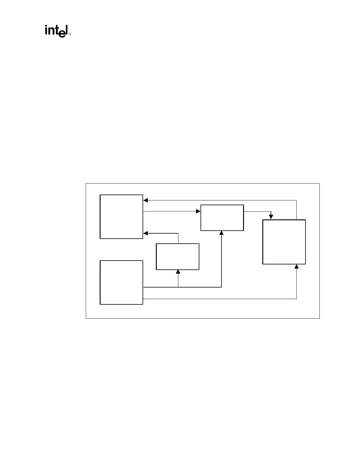
Figure 12-6. VID Routing
VRM
Power
Supply
Processor
VID[4:0]
3.3 VDC
PWR_OK
OUTEN
PWRGD
PWRGOOD
SM_VCC
System
PWRGD
Logic
Delay Logic