Platform Power Delivery Guidelines
176 Design Guide
Use two voltage dividers for each processor, and one for the chipset component. Assume a
maximum of 15 mA of leakage current per load. These leakage currents can be positive or
negative.
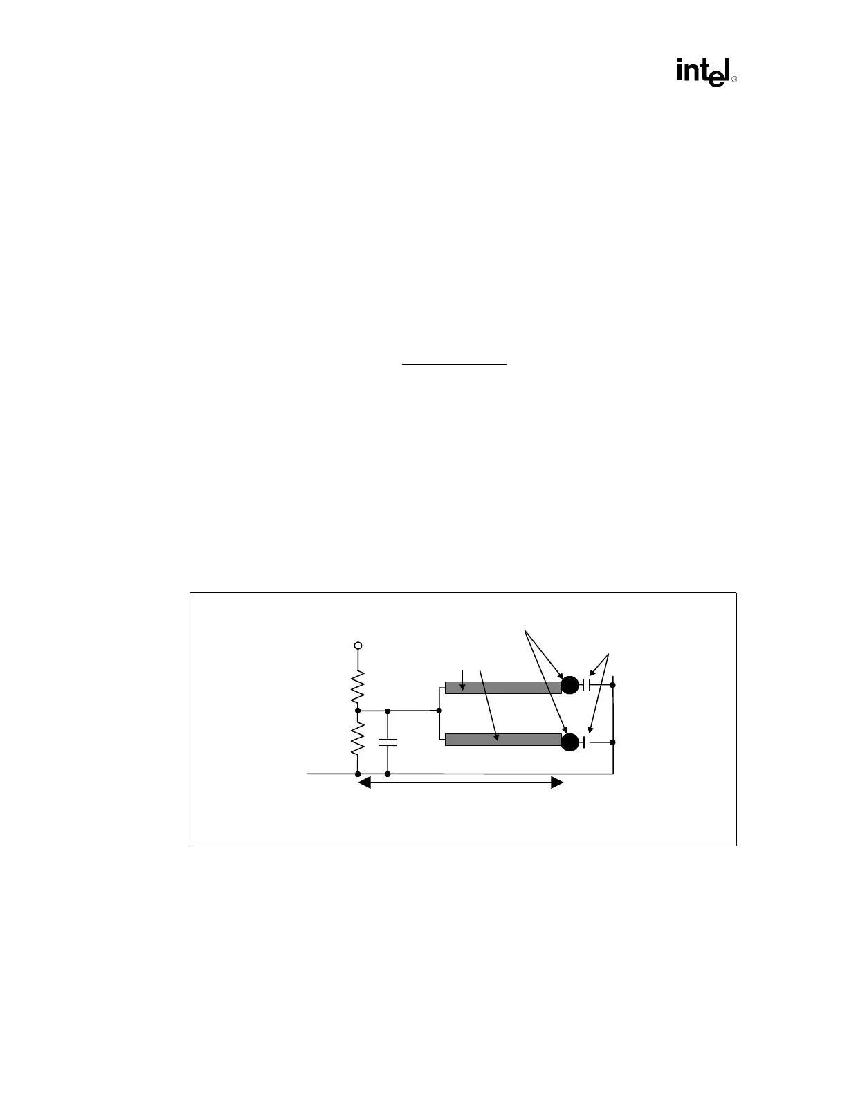
The following discussion illustrates using a single voltage divider to support two GTLREF Loads
assuming VCC_CPU of 1.475 V. Using a 100 Ω ± 1% resistor for R1 and a 49.9 Ω ± 1% resistor
for R2 in Figure 12-14 creates a static usage of 10.7 µA (1.475 V/149.9 Ω) per voltage divider. The
worst case solution for Equation 12-1 can be found with IREF at 30 µA, R1 at the low end of its
tolerance specification (99 Ω), and R2 at the high end of its tolerance specification (50.4 Ω),
yielding Equation 12-2. The target of 2/3 of VCC_CPU is 1.133 V. This resistive setting is within
0.7% of the 2/3 point and satisfies the 2% specification.
Decouple GTLREF[3:0] at each pin with a 220 pF capacitor to VSS. Decoupling GTLREF to VSS
at the voltage dividers with a 1 µF capacitor may further enhance the ability for GTLREF to track
VCC.
When routing GTLREF to the pins, use a 30–50 mil trace (the wider the better), and keep it as short
as possible (less than 1.5 inches). Also, keep all other signals at least 20 mils away from the
GTLREF trace. This provides a low impedance line without the cost of an additional plane or
island. Because of the placement of the GTLREF pins on the processor, it may not be possible or
convenient to route all four pins from one voltage divider. It is acceptable to use more than one
voltage divider with decoupling at each voltage divider and each pin.
Equation 12-2. Resistor Tolerance Analysis
V
EF
= 1.475/50.4 - .000030 = 1.1255V
1/50.4 + 1/99
Figure 12-14. Suggested GTLREF Generation
VCC_CPU
GTLREF
VSS
GTLREF Pins
Baseboard Routing
49 Ω ± 1%, 25 mW
100 Ω ± 1%, 25 mW
1 µF
High Frequency
Capacitors at Each
GTLREF Pin
Routing Distance Between
Voltage Divider and Pin
Should Be Less Than 1.5"