System Bus Routing Guidelines
62 Design Guide
5.3.2.1 Proper Power Good Usage
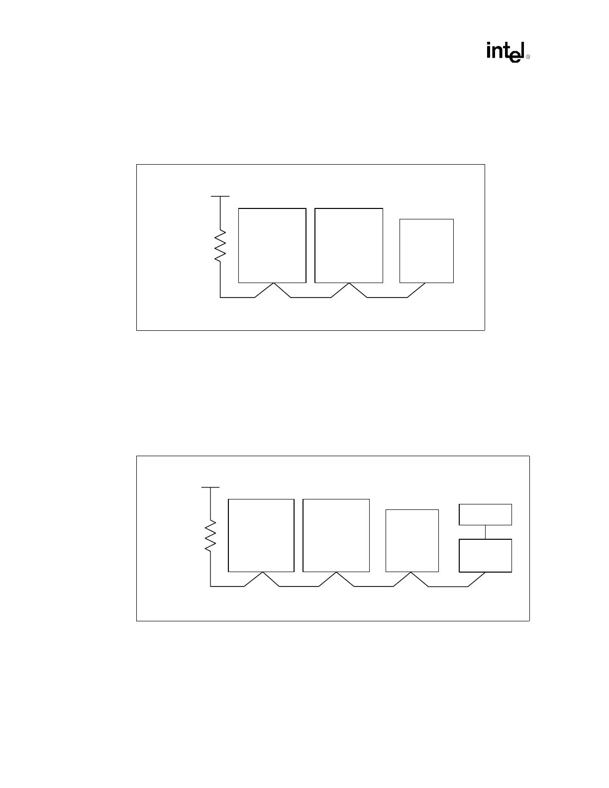
Route CPUPWRGD as shown in Figure 5-7. You may choose to isolate PWRGOOD for each
voltage regulator and processor pair in order to recognize individual voltage regulator failures.
NOTES:
1. Trace Z
0
= 50 Ω.
2. Trace spacing = 10 mil.
5.3.2.2 Voltage Translation for INIT#
A voltage translator circuit is required for the INIT# signal for all platforms that use the FWH. The
required routing topology for INIT# is given in Figure 5-8. Do not route a stub when routing to the
processors. Figure 5-9 shows the voltage translator circuit.
NOTE: The total trace length between the ICH3-S pin and the Processor 0 pin must be less than 15 inches.
Figure 5-7. Topology for PWRGOOD (CPUPWRGOOD)
Intel
®
ICH3-S
Processor 0 Processor 1
0.1" – 3.0"
0.1" – 9.0" 0.1" – 9.0"
VCC_CPU
300 Ω ± 5%
Figure 5-8. INIT# Routing Topology
Intel
®
ICH3-S
Processor 0 Processor 1
0.1" – 3.0"
0.1" – 9.0"
VCC_CPU
200 Ω ± 5%
0.1" – 9.0"
0.1" – 9.0"
Voltage
Translator
FWH