Design Guide 49
Platform Clock Routing Guidelines
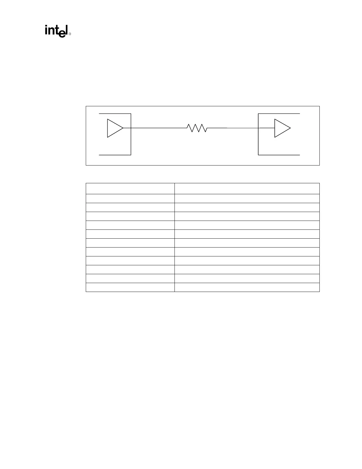
4.1.6 USBCLK Clock Group
For the USBCLK clock group, the driver is the clock synthesizer USB clock output buffer, and the
receiver is the USB clock input buffer at the ICH3-S. Note that this clock is asynchronous to any
other clock on the board.
Figure 4-14. Topology for USB_CLK
Table 4-9. USBCLK Routing Guidelines
Parameter Routing Guideline
Clock Group USBCLK
Topology Point-to-Point
Reference Plane Ground referenced (contiguous over entire length)
Characteristic Trace Impedance (Z
0
) 50 Ω ± 10%
Trace Width 5 mils
Trace Spacing 25 mils
Trace Length – L1 0.00” – 0.50”
Trace Length – L2 3.00” – 12.00”
Resistor R1 = 33
Ω ± 5%
Skew Requirements None – USBCLK is asynchronous to any other clock on the board
Maximum Via Count 2
R1
L1 L2
Intel
®
ICH3-S
Clock
Driver