Platform Clock Routing Guidelines
46 Design Guide
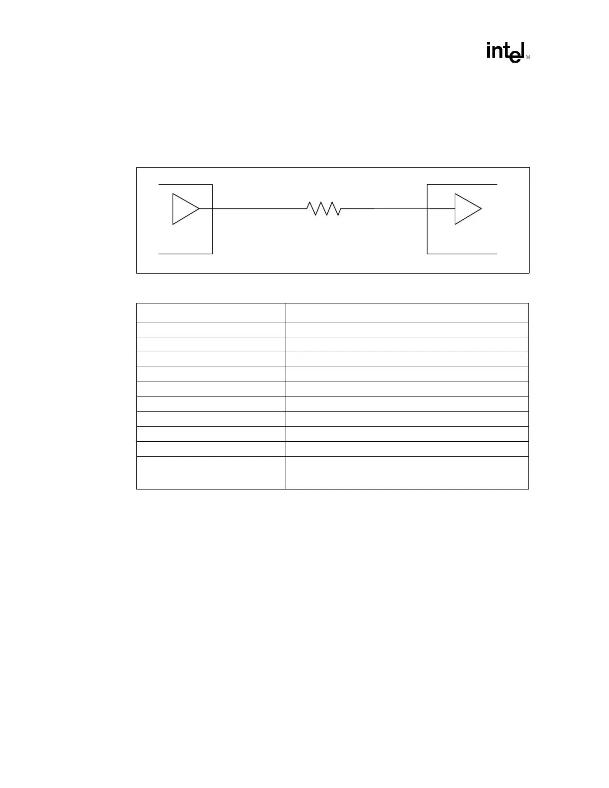
4.1.4 CLK33 Clock Group
For the CLK33 clock group, the driver is the clock synthesizer 33 MHz clock output buffer, and the
receiver is the 33 MHz clock input buffer at the PCI devices on the PCI cards.
.
Figure 4-11. Topology for CLK33 to PCI Device Down
Table 4-6. CLK33 Routing Guidelines for PCI Device Down
Parameter Routing Guidelines
Clock Group CLK33
Topology Point-to-Point
Reference Plane Ground referenced (contiguous over entire length)
Characteristic Trace Impedance (Z
0
) 50 Ω ± 10%
Trace Width 5 mils
Trace Spacing 25 mils
Trace Length – L1 0.00” – 0.50”
Trace Length – L2 3.00” – 9.0”
Resistor R1 = 33
Ω ± 5%
Skew Requirements PCI device – PCI device skew max allowed by
PCI Local Bus
Specification, Rev 2.2
is 2 ns. Therefore, length match with other
CLK33 signals within ± 1 ns.
R1
L1 L2
PCI Device,
FWH, BMC, SIO
Clock
Driver