Design Guide 209
Schematic Checklist
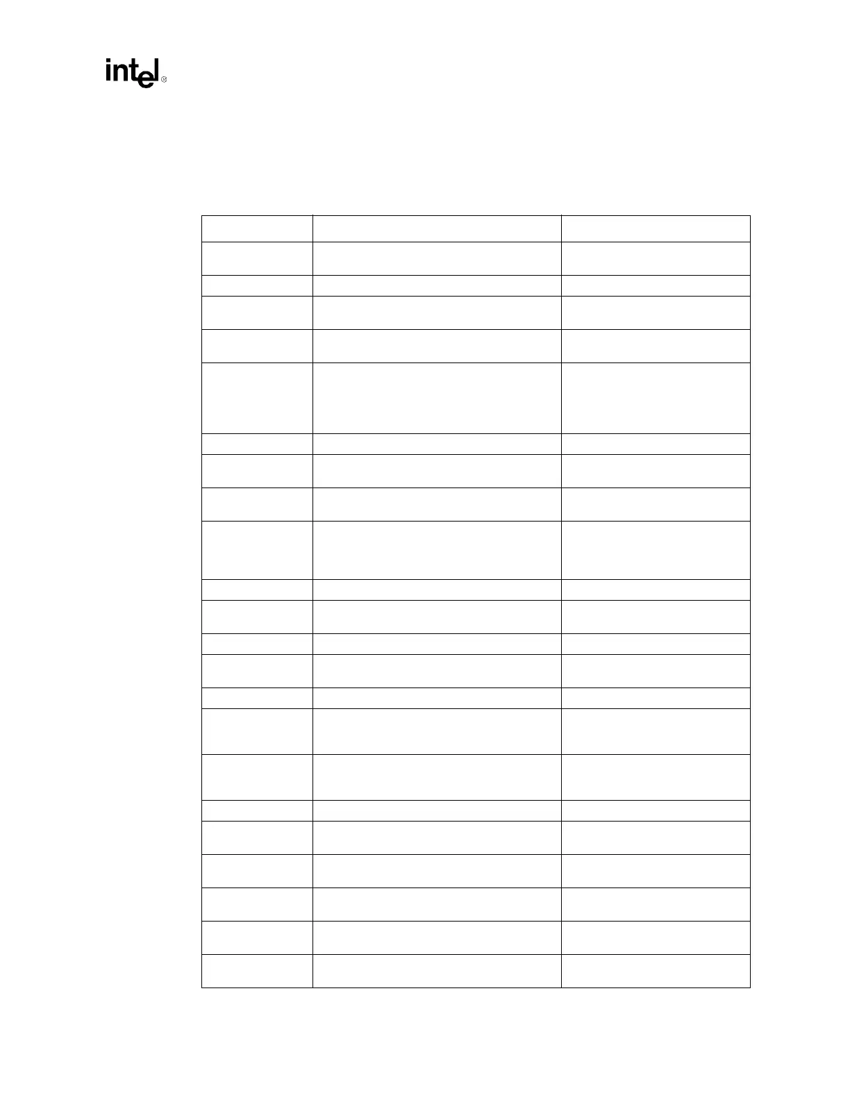
13.5 CK408 Schematic Checklist
Table 13-5. CK408 Schematic Checklist
Checklist Items Recommendations Reason/Impact
66BUFF[2:0] • Connect to a P64H2 using a series
43
Ω ± 5% resistor.
• Refer to Section 4.1.2.
66IN • No Connect.
3V66_0 • Connect to ICH3-S using a series
43
Ω ± 5% resistor.
• Refer to Section 4.1.2.
3V66_1_VCH • Connect to MCH using a series
43
Ω ± 5% resistor.
• Refer to Section 4.1.2.
CPU[3:0]
CPU[3:0]#
• Connect to the processor, MCH, or ITP
using a series 33
Ω ± 5% resistor, and
terminate to GND through a 49.9
Ω ± 1%
resistor. On the ITP port, use a 10 k
Ω ± 5%
pull-up resistor to V3_CLK close to CK408B.
• Refer to Section 4.1.1.
DOT_48MHz • No Connect.
IREF • Terminate to GND through a 475
Ω ± 1%
resistor.
MULT0 • Terminate to V3_CLK through a series
10 k
Ω ± 5% resistor.
PCI[4:0] • Connect to a series 33
Ω ± 5% resistor for
PCI33_CLK33, VIDEO_CLK33,
FWH_CLK33, SIO_CLK33, and
LPC_CLK33.
• Refer to Section 4.1.4.
PCI[6:5] • No Connect.
PCIF[0] • Connect to a series 33
Ω ± 5% resistor for
ICH3_CLK33.
• Refer to Section 4.1.3.
PCIF[2:1] • No Connect.
PCI_STOP# • Terminate to V3_CLK through a 10 k
Ω ± 5%
resistor.
PWRDWN# • Connect to SLP_S3_N.
REF0 • Connect to a series 22
Ω ± 5% resistor for
CLK 14 output to LPC, VIDEO, SIO and
ICH3-S.
• Refer to Section 4.1.5.
SEL[1] • Terminate to V3_CLK through a 10 k
Ω ± 5%
resistor, and terminate to GND through a
10 k
Ω ± 5% resistor.
SCLK, SDTA • Connect to 3V SMBus partition.
USB_48MHz • Connect to ICH3-S using a 33
Ω ± 5%
series resistor to ICH3_CLK48.
• Refer to Section 4.1.6.
VDD, VDD_48MHz
VDDA
• Terminate to V3_CLK_A. • Refer to Section 4.3.
VSS, VSS_48MHz
VSS_IREF
• Terminate to GND. • Refer to Section 4.3.
VTT_PWRGD# • Terminate to GND through 1 k
Ω ± 5%
resistor.
XTAL_IN
XTAL_OUT
• Terminate to GND.