Memory Interface Routing Guidelines
80 Design Guide
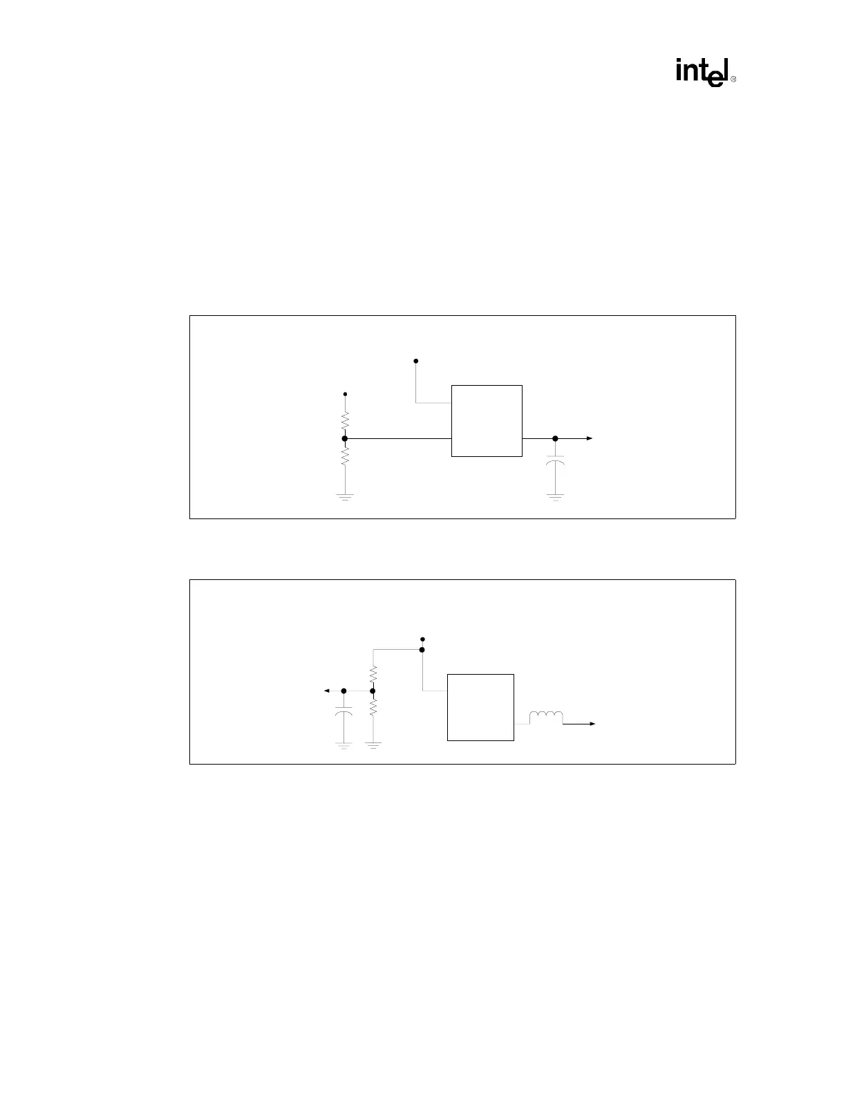
6.9 DDR Reference Voltage
The DDR system memory reference voltage (VREF) is used by the DRAM devices and the MCH
to determine the logic level being driven on the data, strobe, and control signals. VREF of the
receiving device must track changes in VTT to maximize DDR interface margin. If a voltage
regulator is used, it must reference VTT (See Figure 6-16). If a local resistor divider is used, VREF
and VTT must have a common source voltage between them (i.e., both VREF and VTT are derived
from the same voltage plane), and 1% resistors should be used (See Figure 6-17). Decouple VREF
locally at the divider and DIMMs/MCH using one 0.1uF capacitor per VREF pin.
Figure 6-16. DDR VREF Voltage Regulator
DDR VDD
(2.5V)
Voltage
Regulator
DDR VTT
(1.25V)
Vin
Vout
DDR VREF
(1.25V)
Ref
0.1 µF
Figure 6-17. DDR VREF Voltage Divider
Voltage
Regulator
DDR VTT
(1.25V)
Vin
Vout
DDR VREF
(1.25V)
DDR VDD
(2.5V)
1%
1%
0.1 µF