Memory Interface Routing Guidelines
76 Design Guide
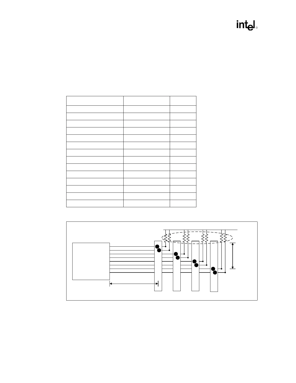
6.5 Chip Select Routing
The MCH provides eight chip select signals. Two chip selects must be routed to each DIMM (one
for each side). The E7500 chip selects for each DIMM must be length matched to the
corresponding clock within ± 2.0 inches and require parallel termination resistors (Rtt) to DDR
VTERM, placed within 3 inches of their associated connector.
NOTES:
1. For 3-DIMM solutions, treat CS6# and CS7# as a no connect.
2. Indicated lengths measure from the MCH pin to the DIMM connector pin, and from the DIMM connector to
the parallel termination resistor pin.
Table 6-6. Chip Select Routing Guidelines
Parameter Intel
®
E7500 Reference
Signal Group CS[7:0]#
Topology Point to Point Figure 6-11
Reference Plane Ground Figure 6-3
Trace Impedance (Zo) 50
Ω ± 10% Figure 6-3
Nominal Trace Width 5 mil Figure 6-3
Nominal Trace Spacing 15 mil Figure 6-3
Trace Length – MCH to DIMM1 1.8” to 9.6” Figure 6-11
Trace Length – MCH to DIMM2 1.8” to 9.6” Figure 6-11
Trace Length – MCH to DIMM3 1.8” to 9.6” Figure 6-11
Trace Length – MCH to DIMM4 1.8” to 9.6” Figure 6-11
Trace Length – DIMM to Rtt < 3.0” Figure 6-11
Termination Resistor (Rtt) 22
Ω ± 2% Figure 6-11
MCH Breakout Guidelines 5/5, < 500 mil
Length Tuning Requirements To CMDCLK pair: ± 2.0” Figure 6-9
Figure 6-11. Chip Select Topology
CS0#
CS1#
CS2#
CS3#
CS4#
CS5#
CS6#
CS7#
MCH
DDR VTERM (1.25V)
DIMMs
Rtt
MCH to DIMM
DIMM
to Rtt