System Bus Routing Guidelines
56 Design Guide
5.1 Routing Guidelines for the AGTL+ Source
Synchronous 2X and 4X Groups
The 4X group of signals uses four times the frequency of the base clock, or 400 MHz. The 2X
group uses twice the frequency of the base clock, or 200 MHz. The 2X and 4X signals are listed in
Table 5-3. Table 5-4 lists the 2X and 4X signals with their associated strobes.
Routing guidelines for the 2X and 4X signal groups are given in Table 5-2. All 2X and 4X signals
of the same group (refer to Table 5-4) must be routed within ± 25 mils of the same length between
agents and within ± 50 mils of the entire length of the bus.
5.1.1 Trace Length Matching
Trace length matching is required within each source synchronous group to compensate for the
package trace length differences between data signals and the associated strobe. This balances the
strobe-to-signal skew in the middle of the setup and hold window. Additional compensation must
be added to account for the capacitive loading effects of the processor socket stubs. Figure 5-2
shows how to implement trace length matching. An example of trace length matching is given in
Example on page 5-57.
Trace length matching consists of matching the pad-to-pad lengths for every signal within a signal
group (e.g., A[35:17]# and ADSTB1#). A pad-to-pad length is measured as follows:
CPU
pad
-to-CPU
pad
= CPU0
pkg_len
+ CPU
pin
-to-CPU
pin
+CPU1
pkg_comp
CPU
pad
-to-MCH
pad
= CPU1
pkg_comp
+ CPU
pin
-to-MCH
pin
+ MCH
pkg_len
Where:
CPU
pin
-to-CPU
pin
= Motherboard trace length between Processor 0 and Processor 1.
CPU
pin
-to-MCH
pin
= Motherboard trace length between Processor 1 and MCH.
pkg_len = Pad to pin length within the package.
0.78 = Compensation due to capacitive loading of processor 1 socket.
CPU1
pkg_comp
= CPUpkg_len * (capacitive loading compensation)
= CPUpkg_len * 0.78
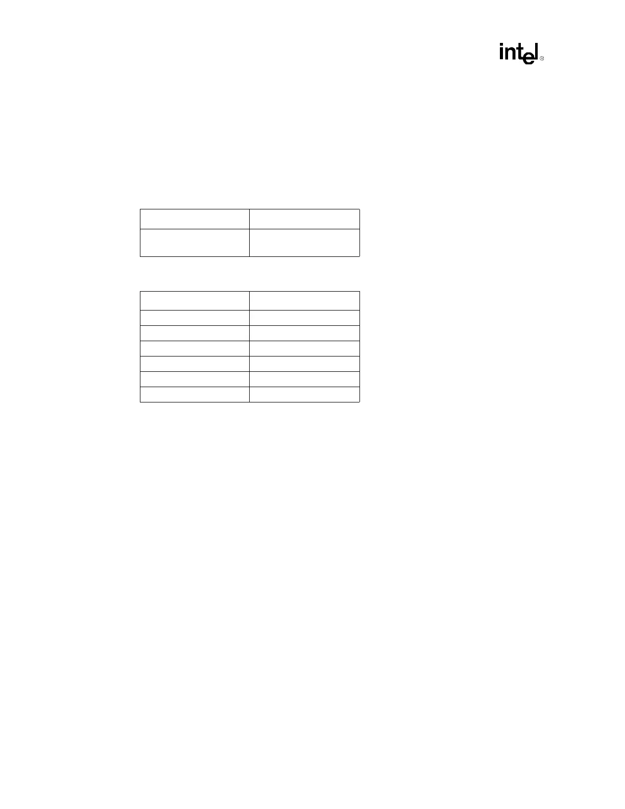
Table 5-3. 2X and 4X Signal Groups
2X Group 4X Group
A[35:3]#
REQ[4:0]#
HD[63:0]#
DBI[3:0]#
Table 5-4. Source Synchronous Signals with the Associated Strobes
Signals Associated Strobe
REQ[4:0]#, HA[16:3]# ADSTB0#
A[35:17]# ADSTB1#
D[15:0]#, DBI0# DSTBP0#, DSTBN0#
D[31:16]#, DBI1# DSTBP1#, DSTBN1#
D[47:32]#, DBI2# DSTBP2#, DSTBN2#
D[63:48]#, DBI3# DSTBP3#, DSTBN3#