Platform Clock Routing Guidelines
42 Design Guide
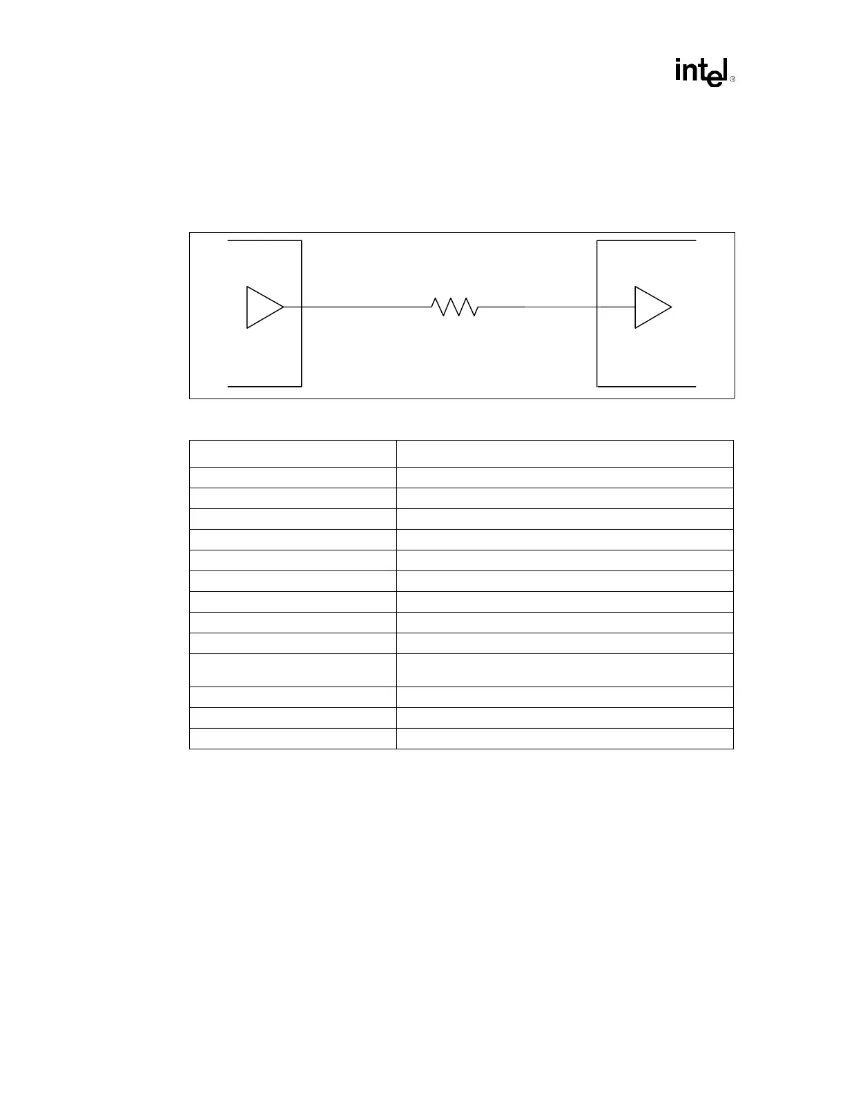
4.1.2 CLK66 Clock Group
In the CLK66 clock group, the driver is the clock synthesizer 66 MHz clock output buffer, and the
receiver is the 66 MHz clock input buffer at the MCH, ICH3-S, and P64H2.
NOTES:
1. For better understanding of the concept, refer to Section 4.1.2.1, Figure 4-7 and Figure 4-8.
2. Assuming no connector.
Figure 4-6. Topology for CLK66
Table 4-4. CLK66 Routing Guidelines
Parameters Routing Guidelines
Clock Group CLK66
Topology Point-to-Point
Reference Plane Ground referenced (contiguous over entire length)
Characteristic Trace Impedance (Z
0
) 50 Ω ± 10%
Trace Width 5 mils
Trace Spacing 25 mils
Trace Length – L1 0.00” – 0.50”
Trace Length – L2 3.00” – 9.0”
Resistor R1 = 43
Ω ± 5%
Skew Requirements
All the clocks in the CLK66 group must have < 100 mil skew
between each other.
Clock Driver to MCH X = (3” – 9.5”)
1
Clock Driver to ICH3-S X = (3” – 9.5”)
Clock Driver to P64H2 X – 0.34”
2
R1
L1 L2
MCH,
Intel
®
ICH3-S,
Intel
®
P64H2
Clock
Driver