Schematic Checklist
204 Design Guide
13.4 Intel
®
82870P2 P64H2 Schematic Checklist
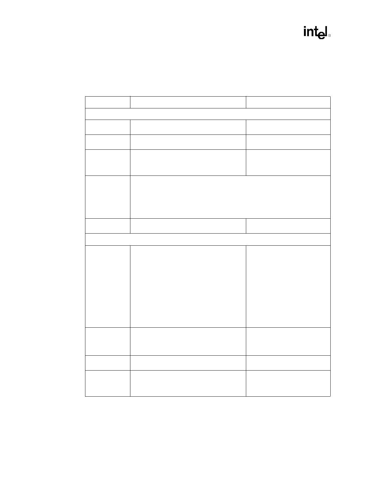
Table 13-4. Intel
®
P64H2 Schematic Checklist (Sheet 1 of 5)
Checklist Items Recommendations Comments
Hub Interface
BPCLK100
BPCLK133
• These can be left as no connects. • These clock signals are used
for testing modes.
CLK200
CLK200#
• If not used, pull-up to VCC3.3 with an
8.2 k
Ω ± 5% resistor.
HI_RCOMP • For a 50
Ω ± 10% board, RCOMP = 61.9 Ω
± 1%. Connect to VCC1.8. The trace length
between the P64H2 pin and the resistor lead
should be < 1".
HI_VREF
HI_VSWING
• P64H2 Hub reference swing voltage = 0.800 V
± 5%.
• R4 = 261
Ω ± 1%, R5 = 332 Ω ± 1%,
R6 = 750
Ω ± 1%.
• C1= 0.1 µF, C2 = 0.01 µF.
• Refer to Figure 7-5 and Figure 7-8.
• Refer to Section 7.2.2 and for
circuit implementation.
HI_[19] • HI[19] can be left as no connect if parity is not
going to be used.
PCI/PCI-X Bus Interface
PxAD[63:32]
PxC/BE#[7:4]
PxDEVSEL#
PxFRAME#
PxIRDY#
PxTRDY#
PxSTOP#
PxPERR#
PxSERR#
PxREQ[5:0]#
PxPLOCK#
PxPAR64
PxACK64#
PxREQ64#
•8.2 k
Ω ± 5% pull-up resistor to VCC3.3. • See PCI Specification Rev 2.2.
PAGNT3# • CLK66 Mode: 8.2 k
Ω ± 5% pull-down to
ground.
• CLK200 Mode: 8.2 k
Ω ± 5% pull-up to
VCC_3.3.
• 1 = Use CLK66.
0 = Use CLK200/CLK200#.
PBGNT3# • Connect to ground through an 8.2 k
Ω ± 5%
pull-down resistor.
GNT[A]#/
GPIO[16]
GNT[B]/ GNT[5]#/
GPIO[17]
• No extra pull-up needed. • These signals have integrated
pull-ups of 24 k
Ω.