Design Guide 71
Memory Interface Routing Guidelines
NOTES:
1. Indicated lengths measure from the MCH pin to the DIMM connector pin (including the series resistor).
Table 6-3. Source Synchronous Signal Group Routing Guidelines
Parameter Intel
®
E7500 Reference
Signal Group DQ[63:0], CB[7:0], DQS[17:0]
Topology Daisy Chain Figure 6-4
Reference Plane Ground Figure 6-3
MCH to Rtt (Zo) 50
Ω ± 10% Figure 6-3
MCH to Rtt Trace Width 5 mil Figure 6-3
Nominal Trace Spacing 15 mil Figure 6-3
Trace Length – MCH to DIMM1 1.8” to 6.0” Figure 6-4
Trace Length – Rs to DIMM1 < 0.8” Figure 6-4
Trace Length – DIMM to DIMM 0.8” to 1.2” Figure 6-4
Trace Length – DIMM to Rtt < 0.8” Figure 6-4
Series Resistor (Rs) 10
Ω ± 2% Figure 6-4
Termination Resistor (Rtt) 22
Ω ± 2% Figure 6-4
MCH Breakout Guidelines 5/5, < 500 mil
Length Tuning Requirements
DQ to DQS: ± 100 mil
DQS to CMDCLK pair: ± 1750 mil
Figure 6-5
Figure 6-6
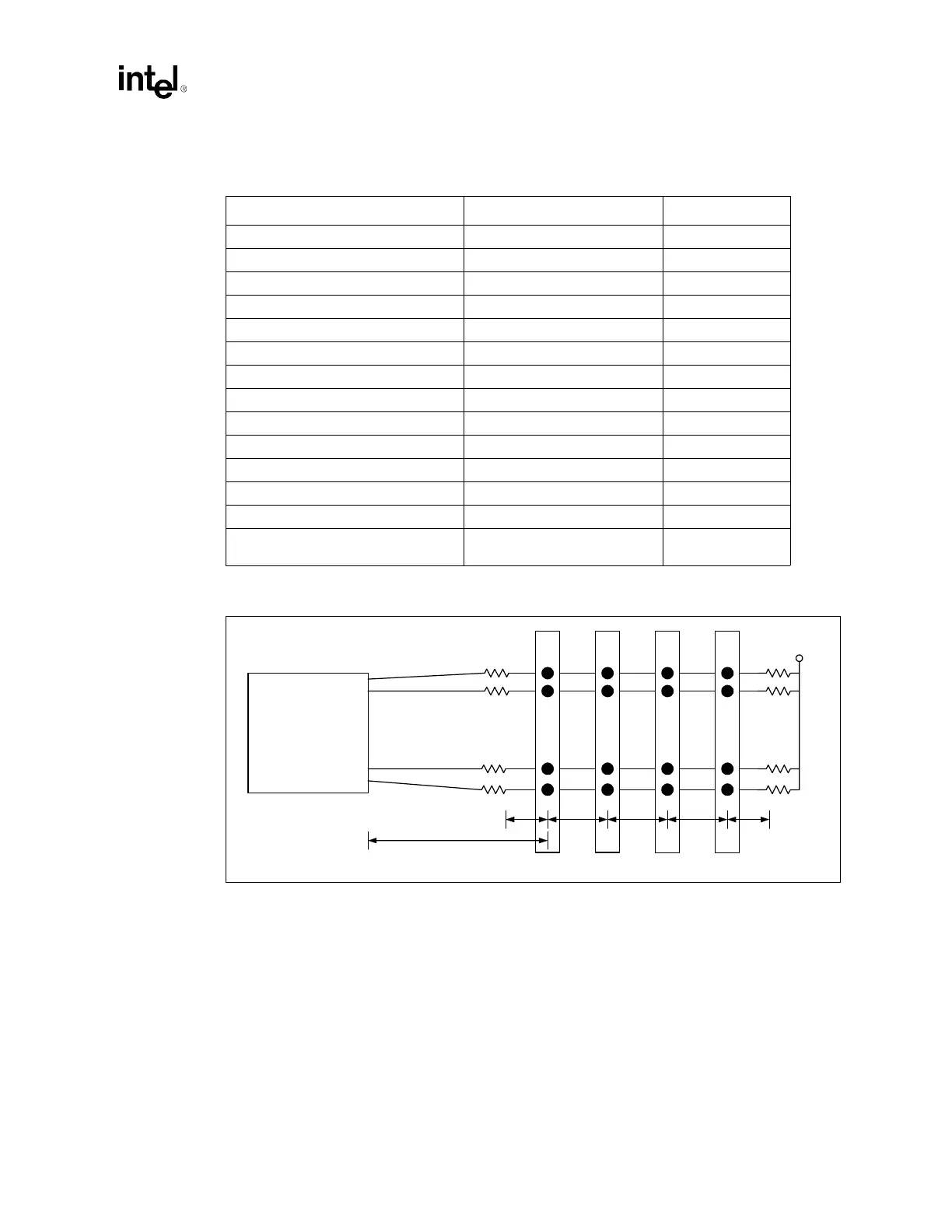
Figure 6-4. Source Synchronous Topology
DIMMs
DQ/CB Data Group
Associated DQS
DQ/CB Data Group
Associated DQS
MCH
DIMM to
DIMM
DDR VTERM
(1.25V)
Intel
®
MCH to DIMM1
Rs
Rs
Rs
Rs
Rtt
Rtt
Rtt
Rtt
Rs to
DIMM1
DIMM to
DIMM
DIMM to
DIMM
DIMM
to Rtt