Design Guide 67
Memory Interface Routing Guidelines
Memory Interface Routing Guidelines 6
The MCH memory interface consists of two DDR memory channels that operate in “lock-step.”
Each channel consists of 64 data and 8 ECC bits. Logically, this is one 144-bit wide memory bus;
electrically, each channel is separate.
This section covers routing guidelines for the DDR interfaces. Note that these guidelines apply to
both channel A and channel B. Each DDR interface has seven signal types: Source Synchronous
Signals, Command Clocks, Source Clocked Signals, Chip Selects, Clock Enable, Receive Enable,
and Miscellaneous. Table 6-1 summarizes the signal groupings. The MCH contains two complete
sets of these signals, one set per channel. Refer to the Intel
®
E7500 Chipset Memory Controller
Hub (MCH) Datasheet for details on the signals listed in Table 6-1.
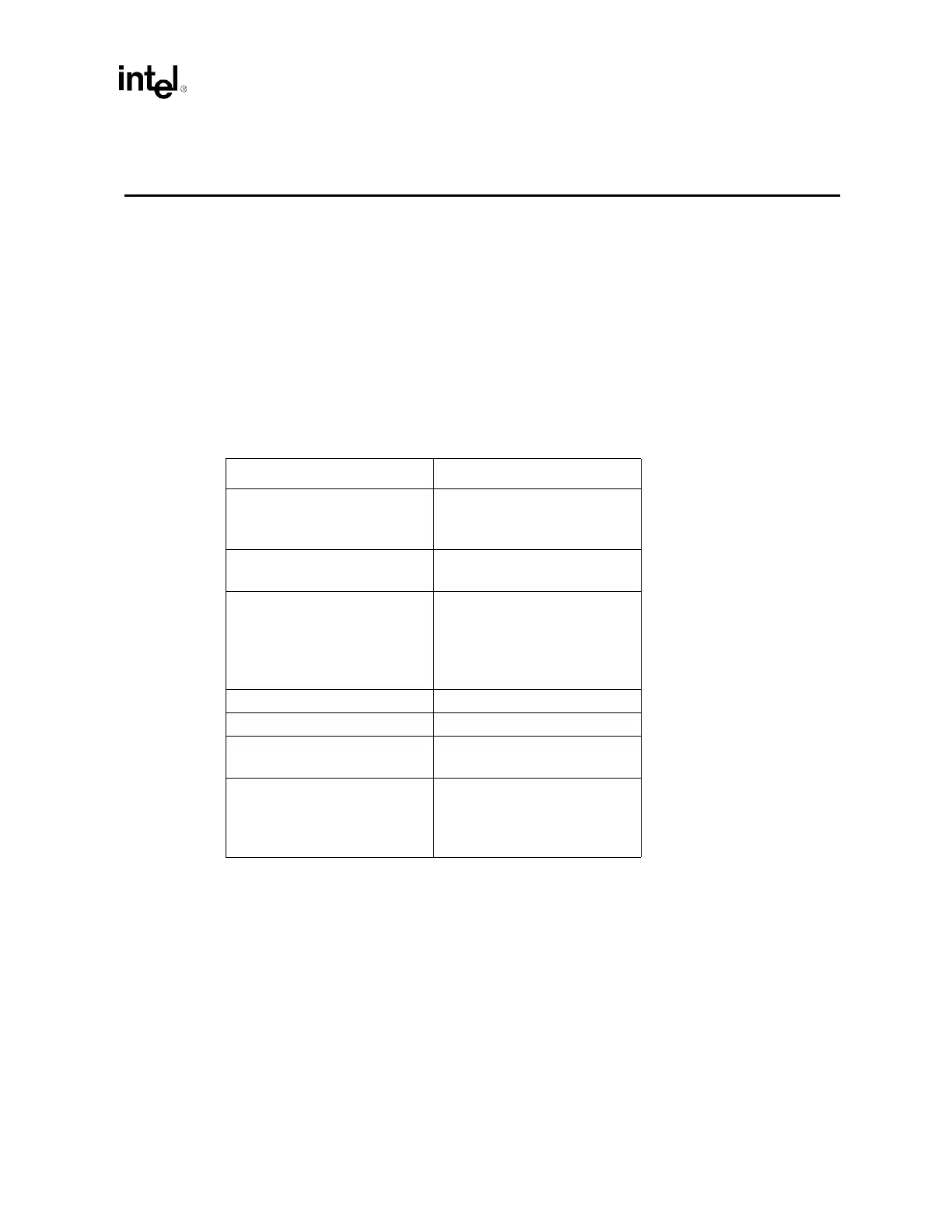
Table 6-1. DDR Channel Signal Groups
Group Signal
Source Synchronous Signals
DQS[17:0]
DQ[63:0]
CB[7:0]
Command Clocks
CMDCLK[3:0]
CMDCLK[3:0]#
Source Clocked Signals
MA[12:0]
RAS#
CAS#
WE#
BA[1:0]
Chip Selects CS#[7:0]
Clock Enable CKE
Receive Enable
RCVENIN#
RCVENOUT#
Miscellaneous
DDRCOMP
DDRCVOH
DDRCVOL
DDRVREF[5:0]