Design Guide 79
Memory Interface Routing Guidelines
6.8 Miscellaneous Signals
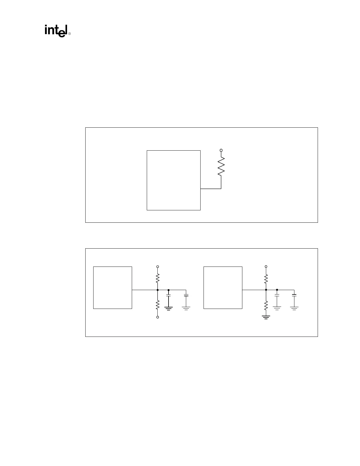
The MCH uses a compensation signal to adjust buffer characteristics and output voltage swing over
temperature, process, and voltage skew. Calibration is done periodically by sampling the
DDRCOMP, DDRCVOH, and DDRCVOL pins on the MCH. Connect DDRCOMP to the DDR
termination voltage (1.25 V) through a 6.81 Ω ± 1% resistor as illustrated in Figure 6-14, and place
the resistor within 1 in. of the MCH. Likewise, keep the voltage divider networks within 1 in. of the
MCH (see Figure 6-15).
Figure 6-14. DDRCOMP Resistive Compensation
MCH
DDR VTERM
(1.25 V)
6.81 Ω ± 1%
<1"
DDRCOMP
Figure 6-15. DDRCVOL and DDRCVOH Resistive Compensation
MCH
DDRCVOH DDRCVOL
DDR VDD
(2.5V)
DDR VTERM
(1.25V)
< 1"
DDR VTERM
(1.25V)
0.01 µF
< 1"
MCH
7 kΩ ± 1%
13 kΩ ±
1%
13 kΩ ± 1%
7 kΩ ±
1%
0.01 µF
0.01 µF
0.01 µF