Design Guide 97
Intel
®
82870P2 (P64H2)
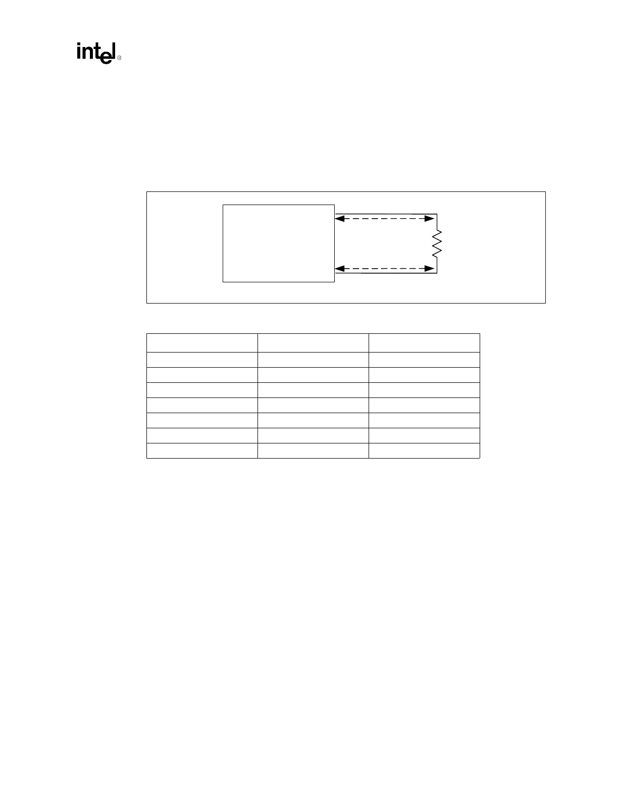
8.1.4 Loop Clock Configuration
You must tie PxPCLKO[6] to PxPCLKI because this clock always runs and is needed by the
internal PCI PLLs to properly align output signals with the external clocks by removing clock
insertion delay. The PxPCLKO[6] signal does not have to be routed through a bus switch before
returning to PxPCLKI.
NOTES:
1. The clock signal and feedback loops are closely related. Refer to Figure 8-4 for L2 and Figure 8-5 for L
fbi
.
Figure 8-5. Loop Clock Configuration
Table 8-6. Loop Clock Configuration Routing Length Parameters
Clock Speed / Config L
fbo
(inches) L
fbi
(inches)
33 MHz / No HP 3.5 – 5.5 2.9 – 7.9
66 MHz / No HP 4.5 – 5.5 3.9 – 4.9
66 MHz / With HP 0.25 – 1.0 7.0 – 12.0
100 MHz / No HP
≤ 1.0 L2 + 2.5
1
100 MHz / With HP 4.5 – 5.5 3.9 – 4.9
133 MHz / No HP 0.25 – 1.0 L2 + 2.5
1
133 MHz / With HP 3.5 – 4.0 5.5 – 5.7
Intel
®
P64H2
33 Ω
PxPCLKO[6]
PxPCLKI
L
fbi
L
fbo