Platform Clock Routing Guidelines
48 Design Guide
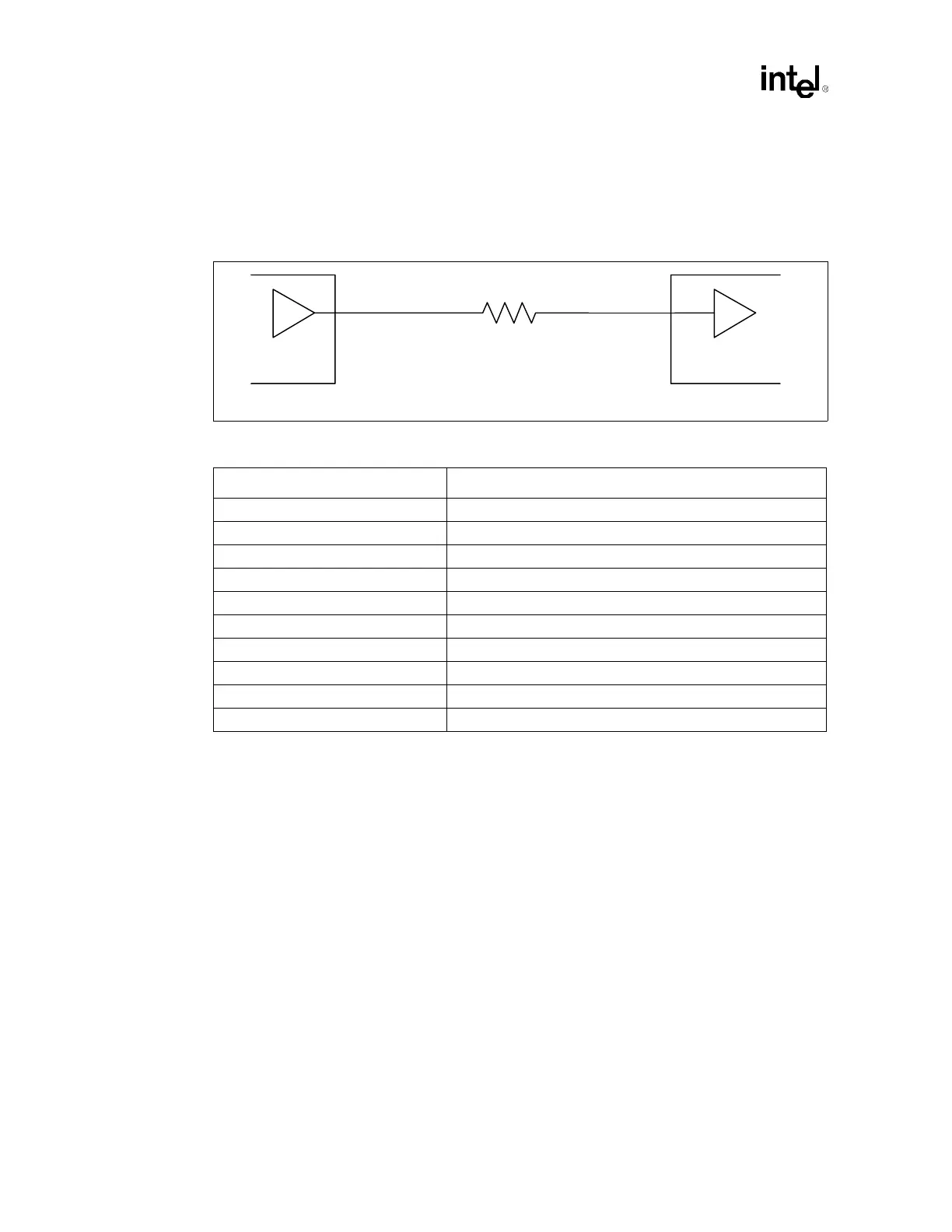
4.1.5 CLK14 Clock Group
The driver in the CLK14 clock group is the clock synthesizer 14.318 MHz clock output buffer, and
the receiver is the 14.318 MHz clock input buffer at the ICH3-S, SIO and LPC.
Figure 4-13. Topology for CLK14
Table 4-8. CLK14 Routing Guidelines
Parameter Routing Guidelines
Clock Group CLK14
Topology Point-to-Point
Reference Plane Ground referenced (contiguous over entire length)
Characteristic Trace Impedance (Z
0
) 50 Ω ± 10%
Trace Width 5 mils
Trace Spacing 10 mils
Trace Length – L1 0.00” – 0.50”
Trace Length – L2 3.00” – 9.0”
Resistor R1 = 22
Ω ± 5%
Skew Requirements None
R1
L1 L2
Intel
®
ICH3-S
SIO, and LPC
Clock
Driver