RL78/G1H CHAPTER 7 TIMER ARRAY UNIT
R01UH0575EJ0120 Rev. 1.20 Page 145 of 920
Dec 22, 2016
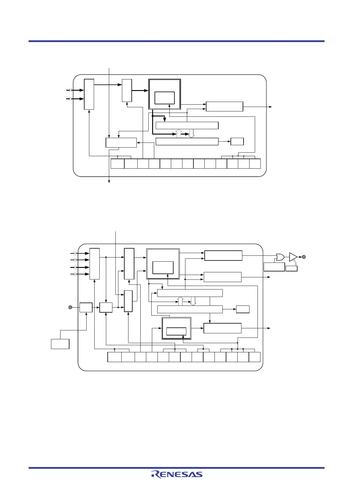
Figure 7 - 4 Internal Block Diagram of Channel 2 of Timer Array Unit 0
Figure 7 - 5 Internal Block Diagram of Channel 3 of Timer Array Unit 0
Mode
selection
Timer
controller
Timer mode register 02 (TMR02)
OVF02
Channel 2
CK00
CK01
Timer counter register 02 (TCR02)
Timer data register 02 (TDR02)
CKS020 CCS02
MAS
TER02
STS022STS021STS020 CIS021 CIS020 MD023 MD022 MD021 MD020
INTTM02 (Timer interrupt)
Interrupt controller
Timer status register 02
(TSR02)
Overflow
fMCK
fTCLK
Operating clock
selection
Count clock
selection
CKS021
Interrupt signal to slave channel
Interrupt signal from master channel
Slave/master
controller
Mode
selection
Timer
controller
INTTM03H (Timer interrupt)
Interrupt controller
Output controller
OVF03
Interrupt controller
CK00
CK01
CK02
CK03
Edge
detection
fMCK
Operating clock
selection
Count clock
selection
Trigger
selection
Interrupt signal from master channel
Timer mode register 03 (TMR03)
CKS030 CCS03
SPLIT
03
STS032STS031STS030 CIS031 CIS030 MD033 MD032 MD031 MD030
Mode
selection
8-bit timer
controller
TO03
INTTM03 (Timer interrupt)
PMxx
Output latch
(Pxx)
Timer status register
03 (TSR03)
Overflow
fTCLK
Channel 3
CKS031
Timer counter register 03 (TCR03)
Timer data register 03 (TDR03)
TI03
Noise
filter
TNFEN03
Noise filter
enable register 1
(NFEN1)
 Loading...


