RL78/G1H CHAPTER 1 OUTLINE
R01UH0575EJ0120 Rev. 1.20 Page 10 of 920
Dec 22, 2016
(2/2)
Note 1. This is about 47 KB when the self-programming function is used (For details, see CHAPTER 4).
Note 2. When using the RF transceiver, pins which a user uses for external connection between the MCU and RF transceiver on
the board are included.
Note 3. The illegal instruction is generated when instruction code FFH is executed.
Reset by the illegal instruction execution is not issued by emulation with the in-circuit emulator or on-chip debug
emulator.
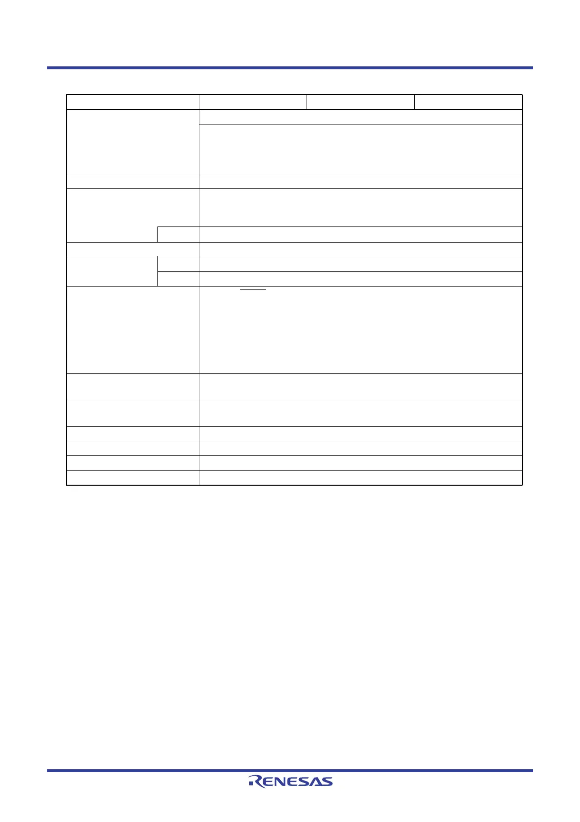
Item R5F11FLJ R5F11FLK R5F11FLL
Clock output/buzzer output 2
• 2.44 kHz, 4.88 kHz, 9.76 kHz, 1.25 MHz, 2.5 MHz, 5 MHz, 10 MHz
(Main system clock: f
MAIN = 20 MHz operation)
• 256 Hz, 512 Hz, 1.024 kHz, 2.048 kHz, 4.096 kHz, 8.192 kHz, 16.384 kHz, 32.768 kHz
(Subsystem clock: f
SUB = 32.768 kHz operation)
10-bit resolution A/D converter 6 channels
Serial interface • CSI/UART: 2 channels
• CSI: 2 channels (1 channel of 2 channels is used for the internal communication between
MCU and RF transceiver.)
I
2
C bus
2 channels
Data transfer controller (DTC) 21 sources
Vectored interrupt
sources
Internal 26
External 7
Reset
• Reset by RESET
pin
• Internal reset by watchdog timer
• Internal reset by power-on-reset
• Internal reset by voltage detector
• Internal reset by illegal instruction execution
Note 3
• Internal reset by RAM parity error
• Internal reset by illegal-memory access
Power-on-reset circuit • Power-on-reset: 1.51 (TYP.)
• Power-down-reset: 1.50 (TYP.)
Voltage detector • Rising edge: 1.88 V to 3.13 V (10 stages)
• Falling edge: 1.84 V to 3.06 V (10 stages)
On-chip debug function Provided
Power supply voltage V
DD = 1.8 to 3.6 V
Operating ambient temperature T
A = -40 to +85 °C (A: Consumer applications, D: Industrial applications)
Package 64-pin HVQFN (9
× 9), (0.5 mm pitch)
 Loading...


