RL78/G1H CHAPTER 14 SERIAL ARRAY UNIT
R01UH0575EJ0120 Rev. 1.20 Page 337 of 920
Dec 22, 2016
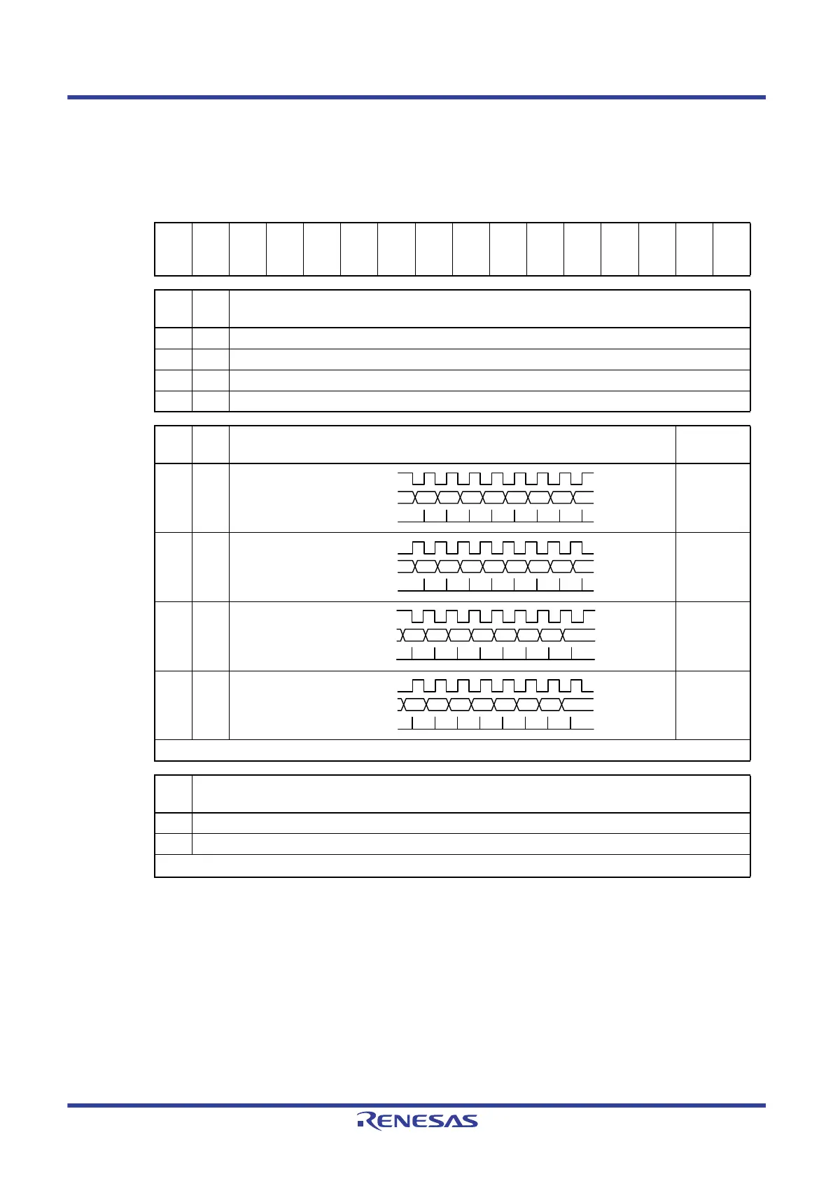
Figure 14 - 8 Format of Serial communication operation setting register mn (SCRmn) (1/2)
Note 1. The SCR02 and SCR12 registers only.
Note 2. When using CSImn not with EOCmn = 0, error interrupt INTSREn may be generated.
Caution Be sure to clear bits 3, 6, and 11 to “0” (Also clear bit 5 of the SCR03, SCR10, SCR11, or SCR13
register to 0). Be sure to set bits 2 and 1 to “1”.
Address: F011CH, F011DH (SCR02), F011EH, F011FH (SCR03), After reset: 0087H R/W
F0158H, F0159H (SCR10)to F015EH, F015FH (SCR13)
Symbol1514131211109876543210
SCRmn
TXE
mn
RXE
mn
DAP
mn
CKP
mn
0
EOC
mn
PTC
mn1
PTC
mn0
DIR
mn
0
SLC
mn1
Note 1
SLC
mn0
011
DLS
mn0
TXE
mn
RXE
mn
Setting of operation mode of channel n
0 0 Disable communication.
0 1 Reception only
1 0 Transmission only
1 1 Transmission/reception
DAP
mn
CKP
mn
Selection of data and clock phase in CSI mode Type
00 1
01 2
10 3
11 4
Be sure to set DAPmn, CKPmn = 0, 0 in the UART mode.
EOC
mn
Mask control of error interrupt signal (INTSREx (x = 1, 3))
0 Disables generation of error interrupt INTSREx (INTSRx is generated).
1 Enables generation of error interrupt INTSREx (INTSRx is not generated if an error occurs).
Set EOCmn = 0 in the CSI mode, and during UART transmission
Note 2
.
D7 D6 D5 D4 D3 D2 D1 D0
SCKp
SOp
SIp input timing
D7 D6 D5 D4 D3 D2 D1 D0
SCKp
SOp
SIp input timing
D7 D6 D5 D4 D3 D2 D1 D0
SCKp
SOp
SIp input timing
D7 D6 D5 D4 D3 D2 D1 D0
SCKp
SOp
SIp input timing
 Loading...


