EasyManua.ls Logo

Renesas RL78/G1H User Manual

Renesas RL78/G1H
941 pages
To Next Page IconTo Next Page
To Previous Page IconTo Previous Page
Page #484 background imageLoading...
Page #484 background image
RL78/G1H CHAPTER 15 SERIAL INTERFACE IICA
R01UH0575EJ0120 Rev. 1.20 Page 466 of 920
Dec 22, 2016
Figure 15 - 31 shows the Communication Reservation Timing.
Figure 15 - 31 Communication Reservation Timing
Remark IICAn: IICA shift register n
STTn: Bit 1 of IICA control register n0 (IICCTLn0)
STDn: Bit 1 of IICA status register n (IICSn)
SPDn: Bit 0 of IICA status register n (IICSn)
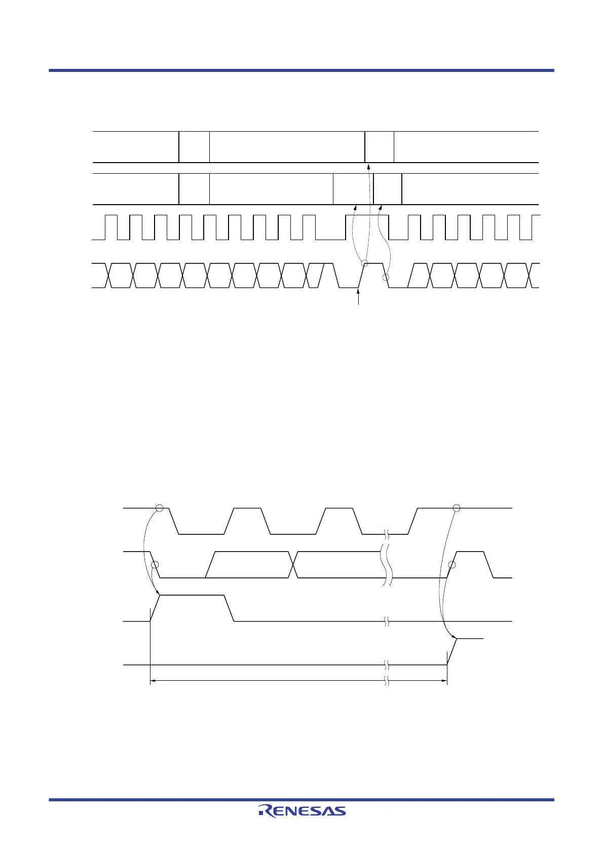
Communication reservations are accepted via the timing shown in Figure 15 - 32. After bit 1 (STDn) of the IICA
status register n (IICSn) is set to 1, a communication reservation can be made by setting bit 1 (STTn) of IICA
control register n0 (IICCTLn0) to 1 before a stop condition is detected.
Figure 15 - 32 Timing for Accepting Communication Reservations
Remark n = 0, 1
1SCLAn
SDAAn
Program processing
Hardware processing
Generate by master device with bus mastership
STTn = 1
Write to
IICAn
Communication
reservation
Set SPDn
and
INTIICAn
Set
STDn
23456789 123456
SCLAn
SDAAn
STDn
SPDn
Standby mode (Communication can be reserved by setting STTn to 1 during this period.)

Table of Contents

Question and Answer IconNeed help?

Do you have a question about the Renesas RL78/G1H and is the answer not in the manual?

Renesas RL78/G1H Specifications

General IconGeneral
Core ArchitectureRL78
Maximum Operating Frequency32 MHz
Flash MemoryUp to 128 KB
Temperature Range-40°C to +85°C
ADC12-bit ADC
Communication InterfacesUART, I2C
D/A ConverterNo
BluetoothNo
PackageLQFP
Timers16-bit Timer x 8, 12-bit Interval Timer x 1

Summary

OUTLINE

Features

Details the key features including low power consumption, CPU core, on-chip RF transceiver, and memory capabilities.

Ordering Information

Provides information on how to order the RL78/G1H microcontroller, including part numbers and package types.

Pin Configuration (Top View)

Illustrates the pin layout of the 64-pin plastic HVQFN package for the RL78/G1H.

Pin Identification

Identifies and describes the function of each MCU and RF transceiver unit pin.

Block Diagram

Shows the overall block diagram of the RL78/G1H, illustrating the MCU and RF parts.

Outline of Functions

Summarizes the key functions of the RL78/G1H, including memory, I/O ports, timers, and RF transceiver.

CONNECTION BETWEEN MCU AND RF TRANSCEIVER

Connection Pins of MCU and RF Transceiver

Lists internal and external pin connections between the MCU and RF transceiver.

Communication Interface Between MCU and RF Transceiver

Details the 3-wire serial I/O (CSI) interface used for internal communication between MCU and RF unit.

Initial Settings of Unused Internal Pins of MCU

Specifies the initial output mode settings for unused internal MCU pins after reset.

Base Operation Clock of RF Unit

Explains the requirement for a 48 MHz clock for RF unit operation and its connection.

Power Configuration

Illustrates the power configuration of the RL78/G1H, including the DC-DC converter for the RF unit.

Peripheral Circuits’Connection Diagram

Provides a diagram showing the connection of peripheral circuits for the RL78/G1H.

PIN FUNCTIONS

Port Functions

Describes the I/O buffer power supplies and pin I/O buffer configurations based on pin types.

Functions other than port pins

Lists functions of pins that are not standard I/O ports, such as analog input, reset, and clock pins.

Connection of Unused Pins

Provides recommended connections for unused pins to prevent floating or unexpected behavior.

Pin Block Diagrams

Illustrates the block diagrams for different pin types, showing internal circuitry.

CPU ARCHITECTURE

Memory Space

Details the 1 MB address space of the RL78/G1H, including program and data memory maps.

Processor Registers

Describes the processor registers, including control registers and general-purpose registers.

PORT FUNCTIONS

Port Functions

Explains the digital I/O ports and their alternate functions, referring to Chapter 3 for details.

Port Configuration

Lists the hardware components related to port configuration, including various registers and port counts.

Registers Controlling Port Function

Lists registers used to control port functions, such as port mode registers and pull-up resistor option registers.

Port Function Operations

Explains port operations, differentiating between output mode and input mode.

Register Settings When Using Alternate Function

Provides basic concepts and examples for setting registers when using alternate pin functions.

Cautions When Using Port Function

Highlights important cautions for using port functions, especially regarding 1-bit manipulation and pin settings.

CLOCK GENERATOR

Functions of Clock Generator

Explains the role of the clock generator in supplying clocks to the CPU and peripheral hardware.

Configuration of Clock Generator

Details the hardware components included in the clock generator.

Registers Controlling Clock Generator

Lists registers used to control the clock generator's operation mode and status.

System Clock Oscillator

Describes the X1 oscillator, XT1 oscillator, high-speed on-chip oscillator, and low-speed on-chip oscillator.

Clock Generator Operation

Explains how the clock generator operates and controls CPU and standby modes.

Controlling Clock

Provides examples and procedures for setting up and controlling various clock sources.

TIMER ARRAY UNIT

Functions of Timer Array Unit

Details the functions of the timer array unit, including independent and simultaneous channel operations.

Configuration of Timer Array Unit

Lists the hardware components included in the timer array unit.

Registers Controlling Timer Array Unit

Lists registers used to control the timer array unit's functions.

Basic Rules of Timer Array Unit

Explains basic rules for simultaneous channel and 8-bit timer operations.

Operation of Counter

Describes how the counter operates, including count clock selection and timing.

Channel Output (TOmn pin) Control

Explains the control of channel outputs to the TOmn pin, including circuit configuration and setting examples.

Timer Input (TImn) Control

Details the TImn input circuit configuration and noise filter usage.

Independent Channel Operation Function of Timer Array Unit

Describes various independent channel operation functions like interval timer and event counter.

Simultaneous Channel Operation Function of Timer Array Unit

Explains simultaneous channel operations, specifically the PWM output function.

Cautions When Using Timer Array Unit

Provides cautions for using timer output and input operations to prevent issues.

TIMER RJ

Functions of Timer RJ

Introduces Timer RJ as a 16-bit timer with reload and down counter, listing its specifications.

Configuration of Timer RJ

Shows the block diagram and configuration of Timer RJ.

Registers Controlling Timer RJ

Lists the registers used to control the Timer RJ peripheral.

Timer RJ Operation

Explains Timer RJ operation modes, reload register, and coordination with ELC.

Cautions for Timer RJ

Provides cautions for using Timer RJ, including start/stop control and mode changes.

REAL-TIME CLOCK

Functions of Real-time Clock

Lists the features of the real-time clock, including counter ranges and interrupt functions.

Configuration of Real-time Clock

Details the hardware components included in the real-time clock.

Registers Controlling Real-time Clock

Lists the registers used to control the real-time clock.

Real-time Clock Operation

Explains the operation of the real-time clock, including starting, stopping, and reading/writing.

12-BIT INTERVAL TIMER

Functions of 12-bit Interval Timer

Describes the interrupt generation at specified time intervals for wakeup and A/D converter SNOOZE mode.

Configuration of 12-bit Interval Timer

Lists the hardware components included in the 12-bit interval timer.

Registers Controlling 12-bit Interval Timer

Lists the registers used to control the 12-bit interval timer.

12-bit Interval Timer Operation

Explains the operation timing of the 12-bit interval timer for generating interrupts.

CLOCK OUTPUT/BUZZER OUTPUT CONTROLLER

Functions of Clock Output/Buzzer Output Controller

Explains the function of the clock output controller for peripheral ICs and buzzer output.

Configuration of Clock Output/Buzzer Output Controller

Lists the hardware components of the clock output/buzzer output controller.

Registers Controlling Clock Output/Buzzer Output Controller

Lists the registers used to control the clock output/buzzer output controller.

Operations of Clock Output/Buzzer Output Controller

Explains the operation of the clock output/buzzer output controller, specifically as an output pin.

Cautions of clock output/buzzer output controller

Provides cautions related to clock output and buzzer output operations.

WATCHDOG TIMER

Functions of Watchdog Timer

Explains the watchdog timer's function in detecting program loops and generating internal reset signals.

Configuration of Watchdog Timer

Details the hardware components of the watchdog timer and how its operation is controlled by the option byte.

Register Controlling Watchdog Timer

Identifies the watchdog timer enable register (WDTE) for controlling the watchdog timer.

Operation of Watchdog Timer

Explains how to control the watchdog timer's operation, including enabling, setting overflow time, and window open period.

A/D CONVERTER

Function of A/D Converter

Describes the A/D converter's function of converting analog input signals to digital values.

Configuration of A/D Converter

Lists the hardware components of the A/D converter.

Registers Controlling A/D Converter

Lists registers used to control the A/D converter's mode, results, and port functions.

A/D Converter Conversion Operations

Explains the A/D converter's conversion operations, including trigger modes and sampling.

Input Voltage and Conversion Results

Shows the relationship between analog input voltage and theoretical A/D conversion results.

A/D Converter Operation Modes

Details various A/D converter operation modes, including software trigger and hardware trigger modes.

A/D Converter Setup Flowchart

Provides flowcharts for setting up software trigger, hardware trigger no-wait, and hardware trigger wait modes.

SNOOZE Mode Function

Explains the SNOOZE mode function for A/D conversion triggered by hardware or ELC events.

Cautions for A/D Converter

Lists important cautions for using the A/D converter, covering operating current, conflicting operations, and noise countermeasures.

SERIAL ARRAY UNIT

Functions of Serial Array Unit

Describes the serial array unit's communication capabilities, including 3-wire serial I/O and UART.

Configuration of Serial Array Unit

Lists the hardware components of the serial array unit.

Registers Controlling Serial Array Unit

Lists registers used to control the serial array unit's functions.

Operation Stop Mode

Explains how to stop the operation of serial array units by units or channels.

Operation of 3-Wire Serial I/O (CSIp) Communication

Details the CSIp communication, including data transfer, clock control, and interrupt functions.

Operation of UART (UARTq) Communication

Explains UART communication, covering data transmission, reception, and error detection.

SERIAL INTERFACE IICA

Functions of Serial Interface IICA

Describes the three modes of serial interface IICA: operation stop, I2C bus, and wakeup modes.

Configuration of Serial Interface IICA

Lists the hardware components of the serial interface IICA.

Registers Controlling Serial Interface IICA

Lists the registers used to control the serial interface IICA.

I2C Bus Mode Functions

Details pin configurations and functions related to the I2C bus mode.

I2C Bus Definitions and Control Methods

Explains I2C bus definitions and control methods, including start conditions, addresses, and ACK.

Timing Charts

Shows timing charts for I2C bus operations, including arbitration and interrupt request timing.

DATA TRANSFER CONTROLLER (DTC)

Functions of DTC

Explains the DTC's function of transferring data between memories without CPU intervention.

Configuration of DTC

Shows the DTC block diagram and its configuration.

Registers Controlling DTC

Lists registers used to control the DTC, including enable, control, and address registers.

DTC Operation

Explains DTC operation modes, including normal and repeat modes, and transfer sizes.

Cautions for DTC

Provides cautions for using the DTC, covering control data allocation and access.

EVENT LINK CONTROLLER (ELC)

Functions of ELC

Describes the ELC's function of linking peripheral events for coordinated operation.

Configuration of ELC

Shows the ELC block diagram.

Registers Controlling ELC

Lists registers used to control the ELC, specifically the event output destination select register.

ELC Operation

Explains the ELC setting procedure for starting and stopping operations.

RF TRANSCEIVER

RF Transceiver Overview

Provides an overview of the RF transceiver, its features, frequency range, and modulation methods.

Pin Functions

Describes the digital and analog pin functions of the RF unit.

Configuration of RF Transceiver

Details the configuration of the RF transceiver, including analog block, digital block, and power supply.

Baseband Function

Explains the baseband function, including configuration, frame control, and interrupts.

Serial Interface Only for Internal Communication

Describes the serial interface used for internal communication between the MCU and RF transceiver.

RF Mode

Classifies the RF operating modes into three types: transmission, reception, and IDLE.

Example of Procedure for Setting

Provides examples of procedures for setting RF parameters like transmission and reception.

Notice For Using Baseband Function

Offers notices and cautions for using the baseband function, particularly regarding transmission and address filters.

INTERRUPT FUNCTIONS

Interrupt Function Types

Describes the two types of interrupt functions: maskable and software interrupts.

Interrupt Sources and Configuration

Lists interrupt sources and their configurations, including reset sources and vector codes.

Registers Controlling Interrupt Functions

Lists registers related to interrupt functions, such as request flags, mask flags, and priority specification flags.

Interrupt Servicing Operations

Explains operations related to interrupt servicing, including acknowledgment and multiple interrupt servicing.

STANDBY FUNCTION

Standby Function

Explains the standby function's purpose of reducing operating current and its three modes: HALT, STOP, and SNOOZE.

Registers controlling standby function

Lists registers that control standby functions, including subsystem clock control and oscillation stabilization registers.

Standby Function Operation

Describes the operating statuses of HALT, STOP, and SNOOZE modes.

RESET FUNCTION

Timing of Reset Operation

Explains the timing of internal reset signals generated by various sources like external reset, POR, and LVD.

Register for Confirming Reset Source

Introduces the reset control flag register (RESF) used to store the source of the reset request.

POWER-ON-RESET CIRCUIT

Functions of Power-on-reset Circuit

Details the functions of the power-on-reset circuit, including generating internal reset signals at power on.

Configuration of Power-on-reset Circuit

Shows the block diagram of the power-on-reset circuit.

Operation of Power-on-reset Circuit

Explains the timing of internal reset signal generation by the power-on-reset circuit and voltage detector.

VOLTAGE DETECTOR

Functions of Voltage Detector

Explains the functions of the voltage detector, including comparing supply voltage with detection voltage.

Configuration of Voltage Detector

Shows the block diagram of the voltage detector.

Registers Controlling Voltage Detector

Lists registers controlling the voltage detector, including voltage detection and level setting registers.

Operation of Voltage Detector

Describes the operation of the voltage detector in different modes (interrupt & reset, reset, interrupt).

Cautions for Voltage Detector

Lists important cautions for using the voltage detector, covering operating current, conflicting operations, and noise countermeasures.

SAFETY FUNCTIONS

Overview of Safety Functions

Provides an overview of safety functions for self-diagnosis and abnormality detection.

Registers Used by Safety Functions

Lists registers used by safety functions, such as CRC control and parity error detection registers.

Operation of Safety Functions

Explains the operation of safety functions like flash memory CRC, RAM parity error detection, and SFR guard.

REGULATOR

Regulator Overview

Provides an overview of the regulator circuit for operating the device with a constant voltage.

OPTION BYTE

Functions of Option Bytes

Explains the functions of option bytes for setting user configurations like watchdog timer and LVD operation.

Format of User Option Byte

Shows the format of the user option byte, detailing settings for flash operation mode and oscillator frequency.

Format of On-chip Debug Option Byte

Describes the format of the on-chip debug option byte for controlling debug operation and security ID.

FLASH MEMORY

Serial Programming Using Flash Memory Programmer

Details serial programming methods using a flash memory programmer or external device.

Connection of Pins on Board

Explains pin connections required for flash memory programming.

Programming Method

Outlines the procedures for writing, erasing, and verifying flash memory.

Processing Time for Each Command When PG-FP5 Is in Use (Reference Value)

Shows processing times for commands when using the PG-FP5 programmer.

Self-Programming

Describes the self-programming function for rewriting flash memory via user programs.

Security Settings

Explains the security function to prohibit rewriting user programs and the relationship between erase/write commands and security.

Data Flash

Provides an overview of the data flash memory and its access methods.

ON-CHIP DEBUG FUNCTION

Connecting E1 On-chip Debugging Emulator

Explains how to connect the E1 on-chip debugging emulator for serial communication.

On-Chip Debug Security ID

Describes the on-chip debug operation control bit and security ID setting area.

Securing of User Resources

Explains the need to secure memory space for debug functions to prevent user program interference.

BCD CORRECTION CIRCUIT

BCD Correction Circuit Function

Explains the function of the BCD correction circuit for obtaining add/subtract result as BCD code.

Registers Used by BCD Correction Circuit

Lists the registers used by the BCD correction circuit.

BCD Correction Circuit Operation

Explains the basic operation of the BCD correction circuit, including addition and subtraction.

INSTRUCTION SET

Conventions Used in Operation List

Defines conventions and symbols used in the operation list for instruction descriptions.

Operation List

Provides a comprehensive list of instructions, their operands, bytes, clocks, and flag operations.

ELECTRICAL SPECIFICATIONS

Absolute Maximum Ratings

Lists the absolute maximum ratings for various parameters like supply voltage and input/output voltage.

Oscillator Characteristics

Details the characteristics of X1 and XT1 oscillators, including frequency ranges and stabilization times.

DC Characteristics

Provides DC characteristics such as output current and input voltage levels.

AC Characteristics

Lists AC timing characteristics for various interfaces like CSI and UART.

Peripheral Functions Characteristics

Describes characteristics of peripheral functions like serial array units and I2C interfaces.

Analog Characteristics

Details analog characteristics, including A/D converter and POR characteristics.

RF Transceiver Characteristics

Covers RF transceiver characteristics, recommended operating conditions, and frequency sets.

RAM Data Retention Characteristics

Specifies RAM data retention characteristics.

Flash Memory Programming Characteristics

Details characteristics related to flash memory programming.

Dedicated Flash Memory Programmer Communication (UART)

Explains communication aspects with the dedicated flash memory programmer via UART.

Timing for Switching Flash Memory Programming Modes

Describes timing for switching between different flash memory programming modes.

PACKAGE DRAWING

APPENDIX A REVISION HISTORY

Major Revisions in This Edition

Lists the major revisions made in the current edition of the manual.

Revision History of Preceding Editions

Provides a history of revisions for previous editions of the manual.

Related product manuals