RL78/G1H CHAPTER 18 RF TRANSCEIVER
R01UH0575EJ0120 Rev. 1.20 Page 659 of 920
Dec 22, 2016
Set initial setting registers in the table below in order from the top in IDLE mode after status <3>.
Setting values for initial setting registers are not depend on “Frequency band identifier” in 31.7.7 Setting values are the
same in cases of crystal oscillation and external clock (TCXO, etc.).
Refer to the latest application note for setting data in Table 18 - 14 when to use the product.
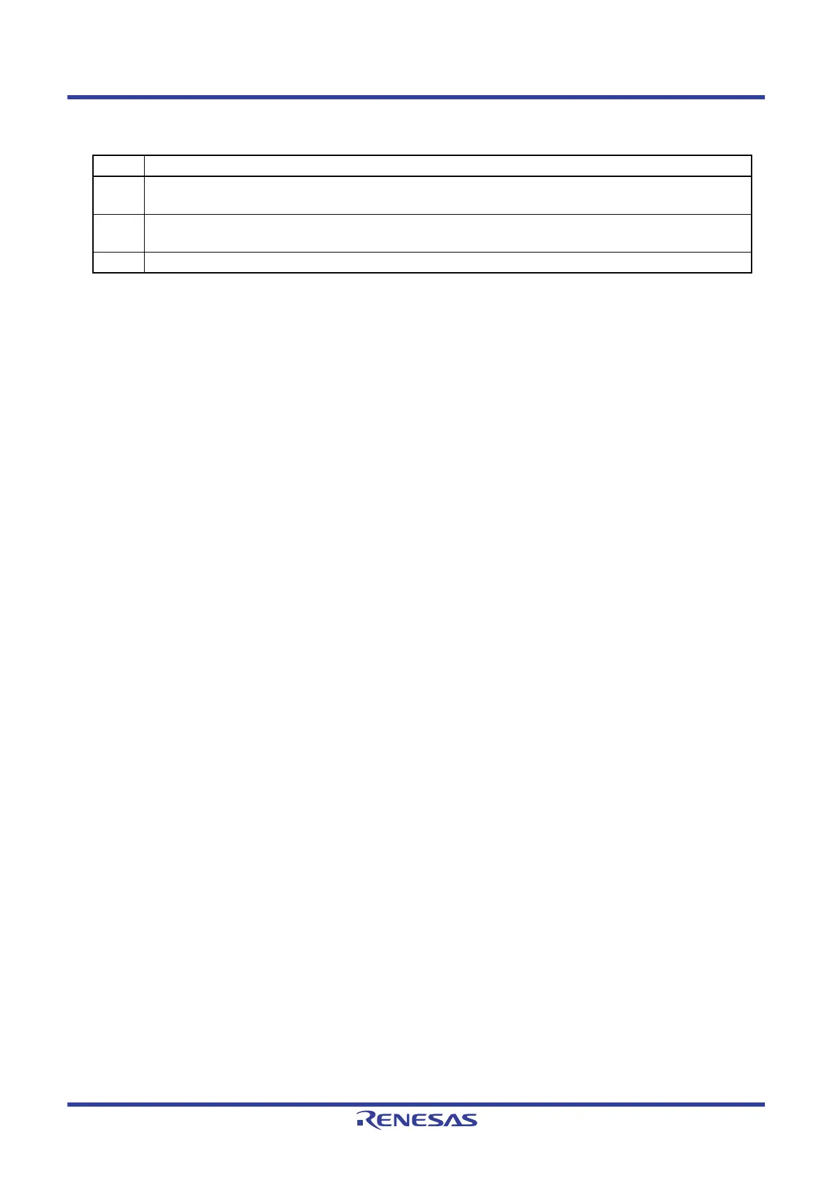
Table 18 - 13 Description of Each State of Wake Up Operation
State Description
<1> Time taken from startup of the XTAL_RF oscillator circuit to the oscillation development.
When the OSCDRVSEL internal pin is at the low level, the buffer size (current) of the oscillator circuit becomes larger.
<2> Time taken from switch of the buffer size of the XTAL_RF oscillator circuit to the output stabilization.
When the OSCDRVSEL internal pin is at the high level, the buffer size (current) of the oscillator circuit is smaller.
<3> Time taken from start of the DC-DC converter operation to the output voltage stabilization.
 Loading...


