RL78/G1H CHAPTER 31 ELECTRICAL SPECIFICATIONS
R01UH0575EJ0120 Rev. 1.20 Page 892 of 920
Dec 22, 2016
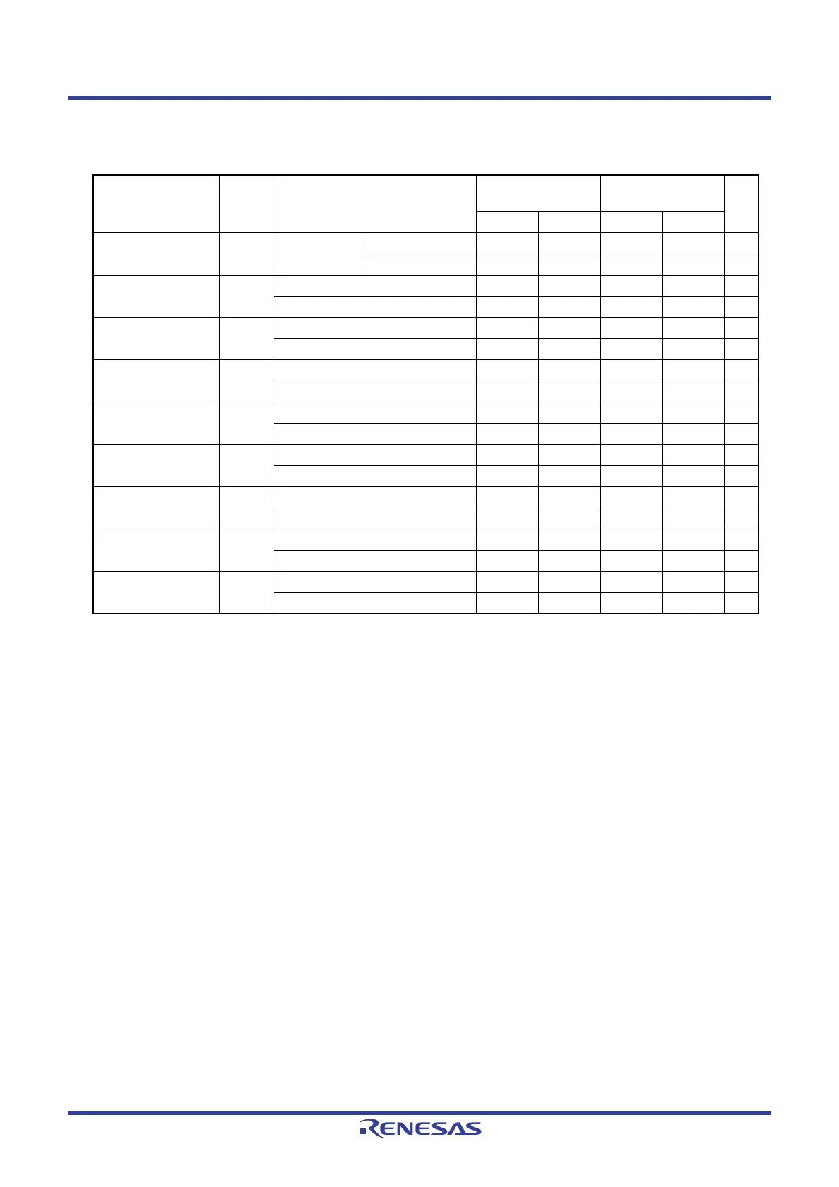
Note 1. The first clock pulse is generated after this period when the start/restart condition is detected.
Note 2. The maximum value (MAX.) of tHD: DAT is during normal transfer and a wait state is inserted in the ACK (acknowledge)
timing.
Remark The maximum value of Cb (communication line capacitance) and the value of Rb (communication line pull-up resistor) at
that time in each mode are as follows.
Fast mode: C
b = 320 pF, Rb = 1.1 kΩ
(2) I
2
C fast mode
(TA = ‒40 to +85 °C, 1.8 V ≤ VDD ≤ 3.6 V, VSS = 0 V)
Parameter Symbol Conditions HS (high-speed main)
mode
LS (low-speed main)
mode
Unit
MIN. MAX. MIN. MAX.
SCLA0 clock frequency f
SCL Fast mode:
f
CLK ≥ 3.5 MHz
2.7 V
≤ VDD ≤ 3.6 V 0 400 0 400 kHz
1.8 V
≤ VDD ≤ 3.6 V 0 400 0 400 kHz
Setup time of restart
condition
t
SU: STA 2.7 V ≤ VDD ≤ 3.6 V 0.6 0.6 μs
1.8 V
≤ VDD ≤ 3.6 V 0.6 0.6 μs
Hold time
Note 1
tHD: STA 2.7 V ≤ VDD ≤ 3.6 V 0.6 0.6 μs
1.8 V
≤ VDD ≤ 3.6 V 0.6 0.6 μs
Hold time when
SCLA0 = “L”
t
LOW 2.7 V ≤ VDD ≤ 3.6 V 1.3 1.3 μs
1.8 V
≤ VDD ≤ 3.6 V 1.3 1.3 μs
Hold time when
SCLA0 = “H”
t
HIGH 2.7 V ≤ VDD ≤ 3.6 V 0.6 0.6 μs
1.8 V
≤ VDD ≤ 3.6 V 0.6 0.6 μs
Data setup time
(reception)
t
SU: DAT 2.7 V ≤ VDD ≤ 3.6 V 100 100 ns
1.8 V
≤ VDD ≤ 3.6 V 100 100 ns
Data hold time
(transmission)
Note 2
tHD: DAT 2.7 V ≤ VDD ≤ 3.6 V 0 0.9 0 0.9 μs
1.8 V
≤ VDD ≤ 3.6 V 0 0.9 0 0.9 μs
Setup time of stop
condition
t
SU: STO 2.7 V ≤ VDD ≤ 3.6 V 0.6 0.6 μs
1.8 V
≤ VDD ≤ 3.6 V 0.6 0.6 μs
Bus-free time t
BUF 2.7 V ≤ VDD ≤ 3.6 V 1.3 1.3 μs
1.8 V
≤ VDD ≤ 3.6 V 1.3 1.3 μs
 Loading...


