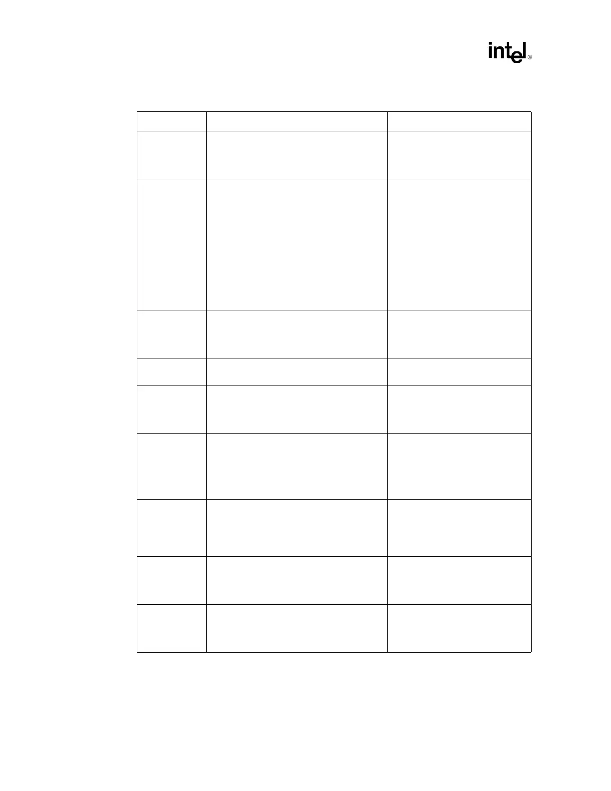
Schematic Checklist
188 Design Guide
BPRI# • Connect to both processors and the MCH. • Used to arbitrate for ownership of
the processor system bus.
• AGTL+ Common Clock Input.
• Refer to Section 5.2.
BR[3:0]# • Connect BR[0]# to the MCH’s BREQ0# pin,
Processor 0’s BR0# pin, and Processor 1’s
BR1# pin. Terminate using a 50
Ω ± 5% pull-
up resistor at Processor 0.
• Connect BR[1]# signal to Processor 0’s
BR1# pin and Processor 1’s BR0# pin.
Terminate both ends of the bus using
50
Ω ± 5% pull-up resistors.
• BR[3:2]# should be terminated individually at
each processor or be connected between
processors and terminated at one end using
a 50
Ω ± 5% pull-up resistor.
• Refer to Figure 5-10 for more clarification.
• Used to arbitrate for ownership of
the processor system bus.
• These signals do not have on-die
processor termination and must
be terminated on the
motherboard.
• BR0# is an AGTL+ Common
Clock I/O.
• BR[3:1]# are AGTL+ Common
Clock Inputs.
• Refer to Section 5.3.6.
COMP[1:0] • Terminate to ground separately using
50
Ω ± 1%.
• Power/Other.
• Sets the processor’s on-die
termination.
• Refer to Section 5.3.5.
D[63:0]#
3
• Connect to both processors and the MCH. • AGTL+ Source Synchronous I/O.
• Refer to Section 5.1.
DBI[3:0]# • Connect to both processors and the MCH. • Indicates the polarity of the
D[63:0]#
3
signals.
• AGTL+ Source Synchronous I/O.
• Refer to Section 5.1.
DBSY# • Connect to both processors and the MCH. • Asserted by the agent responsible
for driving data on the processor
system bus to indicate that the
data bus is in use.
• AGTL+ Common Clock I/O.
• Refer to Section 5.2.
DEFER# • Connect to both processors and the MCH. • Asserted by an agent to indicate
that a transaction cannot be
guaranteed in-order completion.
• AGTL+ Common Clock Input.
• Refer to Section 5.2.
DP[3:0]# • Connect to both processors and the MCH. • Provides parity protection for the
D[63:0]#
3
signals.
• AGTL+ Common Clock I/O.
• Refer to Section 5.2.
DRDY# • Connect to both processors and the MCH. • Asserted by data driver on each
data transfer to indicate valid data.
• AGTL+ Common Clock I/O.
• Refer to Section 5.2.
Table 13-1. Processor Schematic Checklist (Sheet 2 of 6)
Checklist Items Recommendations Comments